EELXT905PC.C2 데이터 시트보기 (PDF) - Intel
부품명
상세내역
제조사
EELXT905PC.C2 Datasheet PDF : 38 Pages
| |||
Universal 10BASE-T Transceiver with 3.3V Support — LXT905
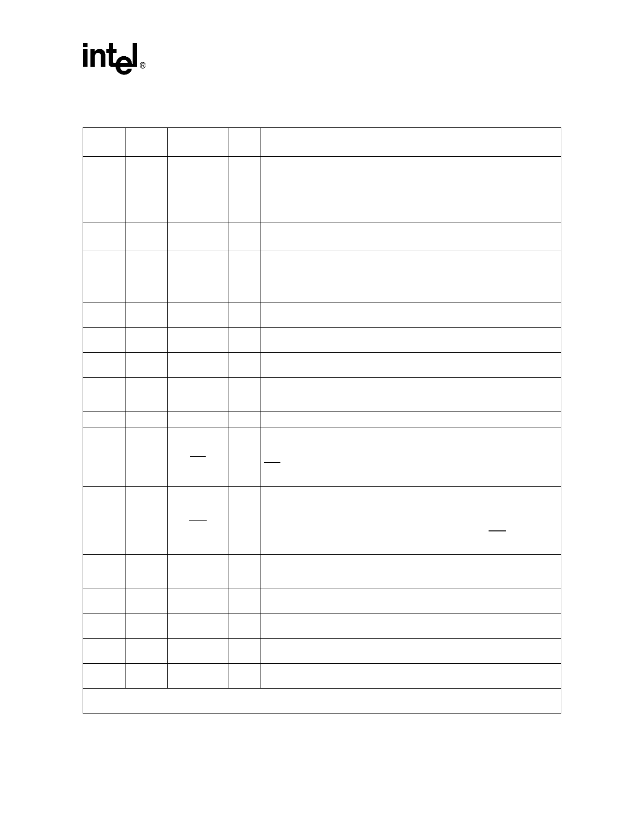
Table 1. LXT905 Signal Descriptions
LQFP
Pin #
PLCC
Pin #
Symbol
I/O
Description
13
1
20
22
27
–
28
–
29
–
VCC1
VCC2
VCC3
VCC4
VCC5
–
–
– Power Inputs 1 thru 5. Power supply inputs of 3.3V or 5V.
–
–
30
2
31
3
CLKI
CLKO
I Crystal Oscillator. A 20 MHz crystal must be connected across these pins, or a
O 20 MHz clock applied at CLKI, with CLKO left open.
11
15
12
23
21
4
32
–
GND1
GND2
GND3
GND4
–
–
Ground.
–
–
1
5
LBK
I
Loopback. When High, forces internal loopback. Disables collision and the
transmission of both data and link pulses. Pulled Low internally1.
2
6
TEN
I
Transmit Enable. Enables data transmission and starts the Watch-Dog Timer
(WDT). Synchronous to TCLK. Pulled Low internally1.
3
7
TCLK
O
Transmit Clock. A 10 MHz clock output. This clock signal should be directly
connected to the transmit clock input of the controller.
4
8
TXD
Transmit Data. Input signal containing NRZ data to be transmitted on the
I network. TXD should be connected directly to the transmit data output of the
controller. Pulled Low internally1.
5
9
COL
O Collision Signal. Output that drives the collision detect input of the controller.
LED Collision or Full-Duplex Enable.
6
10
LEDC/
FDE
O LEDC is an open drain driver for the collision indicator pulls Low during collision.
LED “on” (which is Low output) time is extended by approximately 100 ms.
I
FDE enables full-duplex mode (external loopback) if tied Low externally. Pulled
High internally1.
LED Transmit or Power Down.
LEDT is an open drain driver for the transmit indicator. LED “on” (which is Low
7
11
LEDT/
PDN
O output) time is extended by approximately 100 ms. Output is pulled Low during
I transmit.2
If externally tied Low, the LXT905 goes to power down state (PDN). In power-
down mode, all logic inputs and outputs are tristated.
LED Receive. Open drain driver for the receive indicator LED. LED “on” (i.e.,
8
12
LEDR
O Low output) time is extended by approximately 100 ms. Output is pulled Low
during receive. Pulled High internally1.
9
13
LEDL
O
LED Link. Open drain driver for link integrity indicator. Output is pulled Low
during link test pass. Pulled High internally1.
10
14
CD
O
Carrier Detect. An output for notifying the controller that activity exists on the
network.
14
16
RCLK
O
Receive Clock. A recovered 10 MHz clock that is synchronous to the received
data and connected to the controller receive clock input.
15
17
RXD
O
Receive Data. Output signal connected directly to the receive data input of the
controller.
1. Externally pull-up or pull-down each pin separately using a 10k Ω, 1% termination resistor or tie directly to VCC or ground.
2. Do not allow this pin to float. If unused, tie High.
Datasheet
9
Document #: 249271
Revision #: 002
Rev. Date: June 19, 2001
Share Link: 