CXB1567Q 데이터 시트보기 (PDF) - Sony Semiconductor
부품명
상세내역
제조사
CXB1567Q Datasheet PDF : 16 Pages
| |||
CXB1567Q
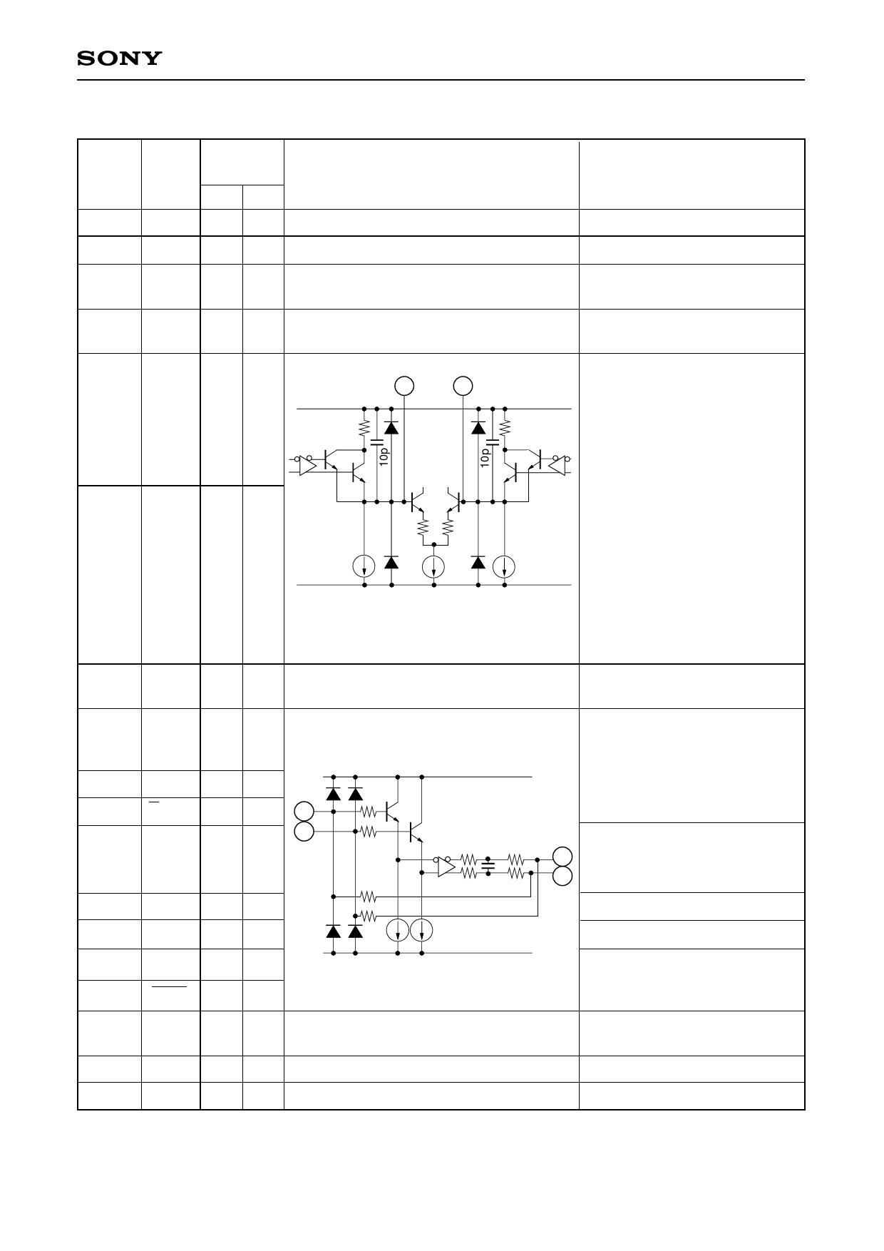
Pin Description
Typical pin
Pin
No.
Symbol voltage (V)
DC AC
1
VEE
–5V
2 N.C.
3
VCCA 0V
4
VEEA –5V
Equivalent circuit
Description
Negative power supply pin.
No connection.
Positive power supply pin for
analog block.
Negative power supply pin for
analog block.
5 CAP3 –1.8V
6 CAP2 –1.8V
5
80
40µA
6
Capacitance connection pins for
VCCA alarm block peak hold circuit.
80
Connect each pin to VCC in
2000pF.
CAP2 pin → Peak hold
capacitance
connection pin for
the limiting
amplifier signal
40µA
CAP3 pin → Peak hold
VEEA
capacitance
connection pin for
the alarm
level setting block
7
VEEA –5V
8D
–0.9V
–1.3V to
–1.7V
9 N.C.
10 D
–1.3V
11 VEEA –5V
100
8
10
100
12 N.C.
1K
13 VEE
–5V
14 N.C.
1K
15 CAP1 –1.8V
16 CAP1 –1.8V
17 to 22 VEED –5V
23, 24 N.C.
25
VEE
–5V
Negative power supply pin for
analog block.
Limiting amplifier input pins
VCCA
Ensure that these inputs are
AC-coupled.
7.5k 130p 200
7.5k 200
VEEA
Negative power supply pin for
16 analog block.
15 No connection.
Negative power supply pin.
No connection.
Capacitance connection pins to
determine the cut-off frequency
for feedback block.
Negative power supply pin for
digital block.
No connection.
Negative power supply pin.
–3–
Share Link: 