PACDN1404(2017) 데이터 시트보기 (PDF) - ON Semiconductor
부품명
상세내역
제조사
PACDN1404 Datasheet PDF : 5 Pages
| |||
PACDN1404
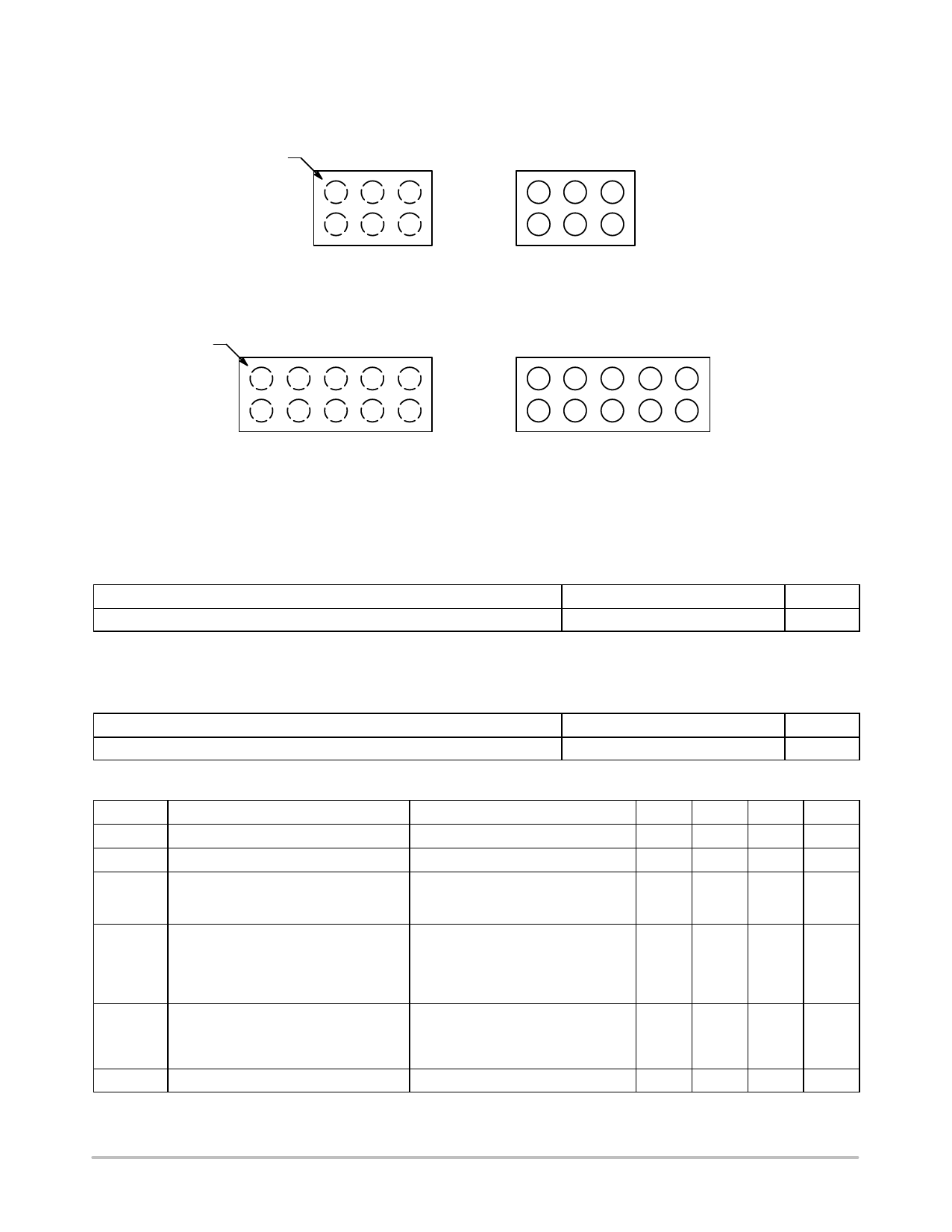
PACKAGE / PINOUT DIAGRAMS
Orientation
Marking
A
B
Top View
(Bumps Down View)
123
+
D14
Bottom View
(Bumps Up View)
B1 B2 B3
A1 A2 A3
PACDN1404
6−Bump WLCSP Package
Orientation
Marking
1
A+
B
Top View
(Bumps Down View)
2345
DN1408
Bottom View
(Bumps Up View)
B1 B2 B3 B4 B5
A1 A2 A3 A4 A5
PACDN1408
10−Bump WLCSP Package
SPECIFICATIONS
Table 1. ABSOLUTE MAXIMUM RATINGS
Parameter
Rating
Units
Storage Temperature Range
−65 to +150
°C
Stresses exceeding those listed in the Maximum Ratings table may damage the device. If any of these limits are exceeded, device functionality
should not be assumed, damage may occur and reliability may be affected.
Table 2. STANDARD OPERATING CONDITIONS
Parameter
Operating Temperature Range
Rating
−40 to +85
Units
°C
Table 3. ELECTRICAL OPERATING CHARACTERISTICS (Note 1)
Symbol
Parameter
Conditions
Min
Typ
Max
VREV
ILEAK
VSIG
Reverse Standoff Voltage
Leakage Current
Signal Clamp Voltage
Positive Clamp
Negative Clamp
IDIODE = 10 mA
VIN = 3.3 V DC
ILOAD = 10 mA
5.5
100
5.6
6.8
8.0
−1.2 −0.8 −0.4
VESD
In−system ESD Withstand Voltage
(Note 2)
a) Human Body Model, MIL−STD−883,
±30
Method 3015
b) Contact Discharge per
±25
IEC 61000−4−2 Level 4
VCL
Clamping Voltage during ESD Discharge (Note 2)
MIL−STD−883 (Method 3015), 8 kV
Positive Transients
+12
Negative Transients
−8
C
Channel Capacitance
At 2.5 V DC, f = 1 MHz
39
47
1. TA = 25°C unless otherwise specified. GND in this document refers to the lower supply voltage.
2. ESD applied to channel pins with respect to GND, one at a time. All other channels are open. All GND pins tied to ground.
Units
V
nA
V
kV
V
pF
www.onsemi.com
2
Share Link: 