LCDA24TE 데이터 시트보기 (PDF) - Semtech Corporation
부품명
상세내역
제조사
LCDA24TE Datasheet PDF : 7 Pages
| |||
LCDA05 THRU LCDA24
PROTECTION PRODUCTS
Applications Information
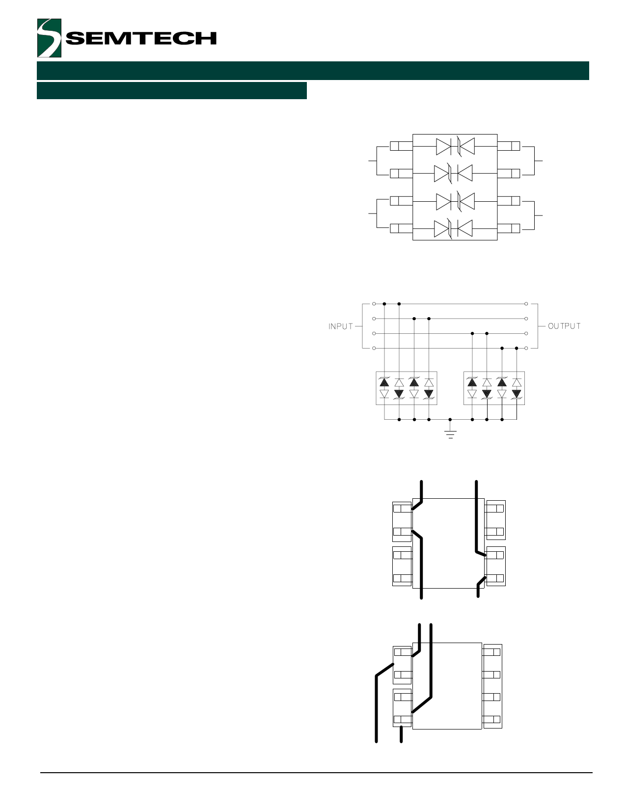
Device Connection for Protection of Two High-Speed
Data Lines
The LCDAxx is designed to protect up to two high-speed
data lines. The LCDAxx utilizes a low capacitance
compensation diode in series with, but in opposite
polarity to a TVS diode in each line. The resulting
capacitance is less than 5pF per line. Each line will
only suppress transient events in one polarity. There-
fore, to achieve protection in both positive and nega-
tive polarity, a second TVS/rectifier pair is connected in
anti-parallel to the first. Pins 1, 2, 7, and 8 are used to
protect one data line. Pins 3, 4, 5, and 6 are used to
protect the second data line.
The device is connected as follows:
l Pins 1 & 2 are tied together and pins 7 & 8 are tied
together providing the protection circuit for one I/O
line. Pins 3 & 4 are tied together and pins 5 & 6
are tied together providing the protection circuit for
the second I/O line. Since the device is electrically
symmetrical, either side of the connected pairs
may be used to protect the lines. The other side of
the pair is used to make the ground connection.
The ground connections should be made directly to
the ground plane for best results. The path length
is kept as short as possible to reduce the effects
of parasitic inductance in the board traces.
Circuit Board Layout Recommendations for Suppres-
sion of ESD.
Good circuit board layout is critical for the suppression
of ESD induced transients. The following guidelines are
recommended:
l Place the TVS near the input terminals or connec-
tors to restrict transient coupling.
l Minimize the path length between the TVS and the
protected line.
l Minimize all conductive loops including power and
ground loops.
l The ESD transient return path to ground should be
kept as short as possible.
l Never run critical signals near board edges.
l Use ground planes whenever possible.
ã 2000 Semtech Corp.
5
LCDA Connection Diagram
1
I/O 1
2
3
I/O 2
4
8
I/O 1
7
6
I/O 2
5
I/O Line Protection
Connection Options
To Protected
Device
1
Line 1
In/Out
2
8
Line 1
Ground
7
3
Line 2
Ground
4
6
Line 2
In/Out
5
Line 1 1
In/Out
2
3
4
From Connector
To Protected
Device
8
Line 2
In/Out
7
Ground
6
5
From Connector
www.semtech.com
Share Link: 