AD1846 데이터 시트보기 (PDF) - Analog Devices
부품명
상세내역
제조사
AD1846 Datasheet PDF : 28 Pages
| |||
AD1846
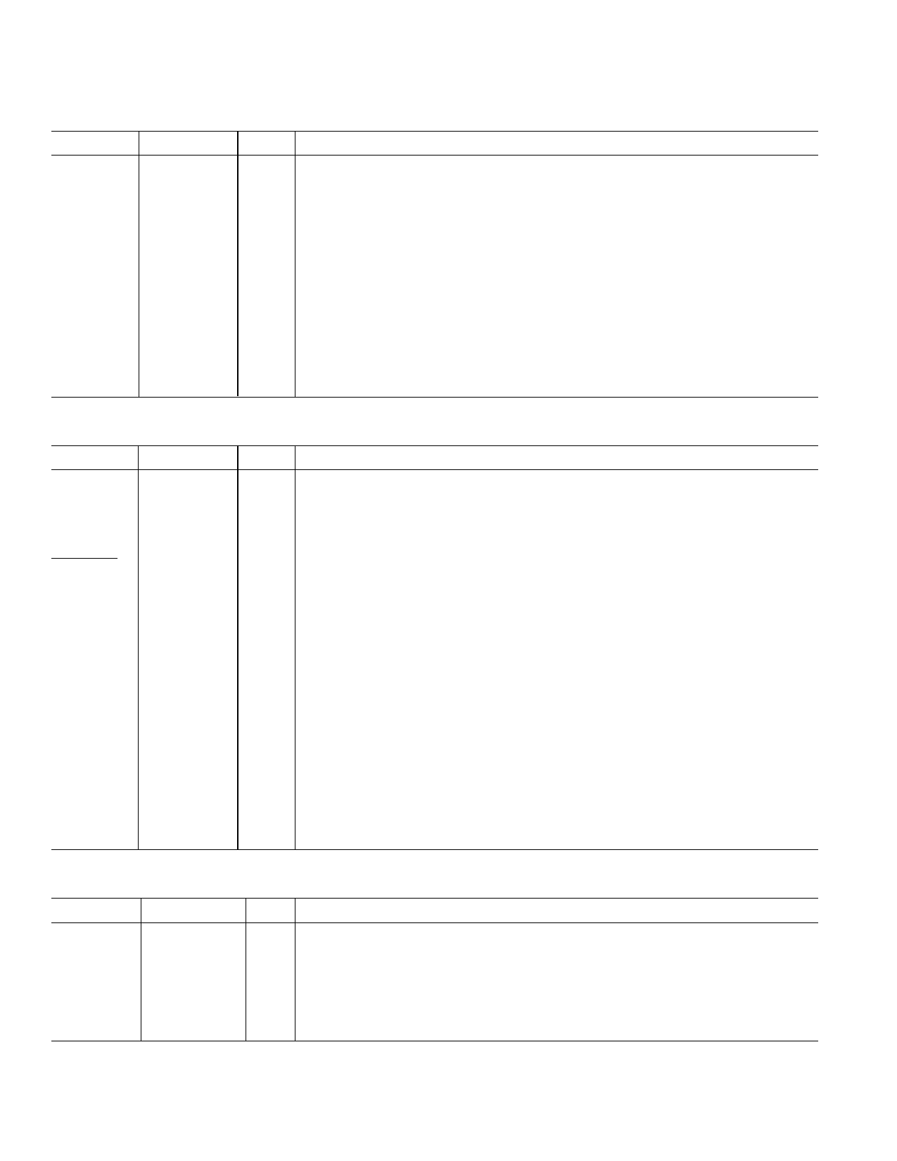
Analog Signals
Pin Name
PLCC
L_LINE
30
R_LINE
27
L_MIC
29
R_MIC
28
L_AUX1
39
R_AUX1
42
L_AUX2
38
R_AUX2
43
L_OUT
40
R_OUT
41
I/O Description
I
Left Line Input. Line level input for the left channel.
I
Right Line Input. Line level input for the right channel.
I
Left Microphone Input. Microphone input for the left channel. This signal can be ei-
ther line level or –20 dB from line level.
I
Right Microphone Input. Microphone input for the right channel. This signal can be
either line level or –20 dB from line level.
I
Left Auxiliary #1 Line Input
I
Right Auxiliary #1 Line Input
I
Left Auxiliary #2 Line Input
I
Right Auxiliary #2 Line Input
O
Left Line Level Output
O
Right Line Level Output
Miscellaneous
Pin Name
XTAL1I
XTAL1O
XTAL2I
XTAL2O
PWRDWN
PLCC
17
18
21
22
23
INT
XCTL1:O
57
56 & 58
VREF
VREF_F
L_FILT
R_FILT
NC
32
33
31
26
46–52, 55
I/O Description
I
24.576 MHz Crystal #1 Input
O
24.576 MHz Crystal #1 Output
I
16.9344 MHz Crystal #2 Input
O
16.9344 MHz Crystal #2 Output
I
Power-Down Signal. Active LO control places AD1846 in its lowest power consump-
tion mode. All sections of the AD1846, including the digital interface, are shut down
and consume minimal power.
O
Host Interrupt Pin. This signal is used to notify the host that the DMA Current Count
Register has underflowed.
O
External Control. These signals reflect the current status of register bits inside the
AD1846. They can be used for signaling or to control external logic. XLTL1 and
XLTL0 are open-drain outputs.
O
Voltage Reference. Nominal 2.25 volt reference available externally for dc-coupling and
level-shifting. VREF should not be used where it will sink or source current.
I
Voltage Reference Filter. Voltage reference filter point for external bypassing only.
I
Left Channel Filter Input. This pin requires a 1.0 µF capacitor to analog ground for
proper operation.
I
Right Channel Filter Input. This pin requires a 1.0 µF capacitor to analog ground for
proper operation.
No Connect. Do not connect.
Power Supplies
Pin Name
PLCC
I/O
VCC
GNDA
VDD
GNDD
35 & 36
I
34 & 37
I
1, 7, 15, 19, I
24, 45, 54
2, 8, 16, 20, I
25, 44, 53, 64
Description
Analog Supply Voltage (+5 V)
Analog Ground
Digital Supply Voltage (+5 V)
Digital Ground
–8–
REV. A
Share Link: 