MAX9937(2008) 데이터 시트보기 (PDF) - Maxim Integrated
부품명
상세내역
제조사
MAX9937
(Rev.:2008)
(Rev.:2008)
Maxim Integrated

MAX9937 Datasheet PDF : 11 Pages
| |||
Automotive Current-Sense Amplifier
with Reverse-Battery Protection
ABSOLUTE MAXIMUM RATINGS
RSP, RSN to GND Voltage Continuous ..................-0.3V to +30V
RSP, RSN to GND Load-Dump Voltage Duration
(VBAT = 40V) with Typical Application Circuit .......................1s
RSP, RSN to GND Reverse-Battery Voltage Duration
(VBAT = -20V) with Typical Application Circuit........Continuous
Differential Input Voltage (RSP - RSN)................................±0.3V
VCC to GND ...........................................................-0.3V to +6.0V
OUT to GND ...............................................-0.3V to (VCC + 0.3V)
Output Short Circuit to Ground ..................................Continuous
Continuous Input Current into RSN, RSP* ........................±50mA
Continuous Input Current into OUT*.................................±25mA
Thermal Limits (Note 1)
5 SC70 Multiple-Layer PCB
Continuous Power Dissipation (TA = +70°C)
(derate 3.1mW/°C above +70°C) ............................246.9mW
θJA ...............................................................................324°C/W
θJC...............................................................................115°C/W
Operating Temperature Range .........................-40°C to +125°C
Junction Temperature ......................................................+150°C
Lead Temperature (soldering, 10s) .................................+300°C
Lead Temperature (reflow) ..............................................+260°C
Note 1: Package thermal resistances were obtained using the method described in JEDEC specification JESD51-7, using a 4-layer
board. For detailed information on package thermal considerations, refer to www.maxim-ic.com/thermal-tutorial.
*Junction temperature rating due to power dissipation must also be observed.
Stresses beyond those listed under “Absolute Maximum Ratings” may cause permanent damage to the device. These are stress ratings only, and functional
operation of the device at these or any other conditions beyond those indicated in the operational sections of the specifications is not implied. Exposure to
absolute maximum rating conditions for extended periods may affect device reliability.
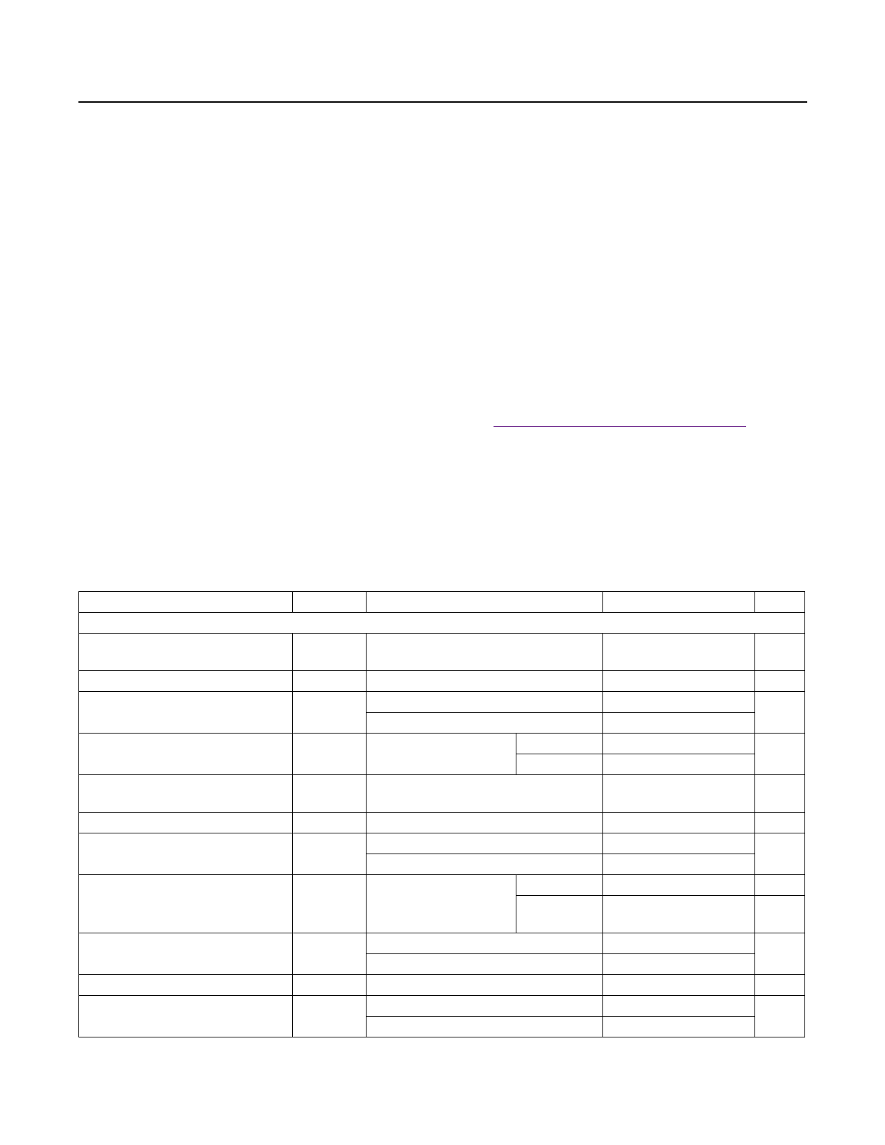
ELECTRICAL CHARACTERISTICS
(VCC = 5V, VBAT = VRS+ = 12V, VSENSE = (VRS+ - VRS-) = 0, RRSP = RRSN = 500Ω, ROUT = 10kΩ, TA = -40°C to +125°C. Typical
values are at TA = +25°C, unless otherwise noted. See the Typical Application Circuit.) (Note 2)
PARAMETER
DC CHARACTERISTICS
Input Common-Mode Voltage
Range
Supply Voltage Range
Input Offset Voltage (Note 3)
Common-Mode Rejection Ratio
Power-Supply Rejection Ratio
Quiescent Supply Current
Input Bias Current (Note 4)
Input Bias Current Mismatch
Input Current in Shutdown
Voltage Gain
Voltage Gain Error (Notes 3, 5)
SYMBOL
CONDITIONS
VRSP,
VRSN
Inferred from CMRR test
VCC
VOS
CMRR
PSRR
ICC
IB+, IB-
ΔIB / IB
Inferred from PSRR test
TA = +25°C
TA = -40°C to +125°C
VBAT = +4V to +28V
TA = +25°C
TA = +125°C
VCC = +2.7V to +5.5V
VCC = 5V
TA = +25°C
TA = -40°C to +125°C
TA = +25°C
2 x (IB+ - IB-)/(IB++IB-) TA = -40°C to
+125°C
IRSP + IRSN
TA = +25°C, VCC = 0
TA = -40°C to +125°C, VCC = 0
Gain = ROUT/RRSP
TA = +25°C
TA = -40°C to +125°C
MIN TYP MAX UNITS
4
28
V
2.7
5.5
V
±0.3 ±1.2
mV
±1.6
100
120
dB
90
90
120
dB
20
55
µA
0.8
2
5.6
µA
0.65
6.5
±1
±12
%
±15
%
0.01
1
µA
10
20
V/V
±0.2 ±1.5
%
±2.0
2 _______________________________________________________________________________________
Share Link: