NCP4586 데이터 시트보기 (PDF) - ON Semiconductor
부품명
상세내역
제조사
NCP4586 Datasheet PDF : 18 Pages
| |||
NCP4586
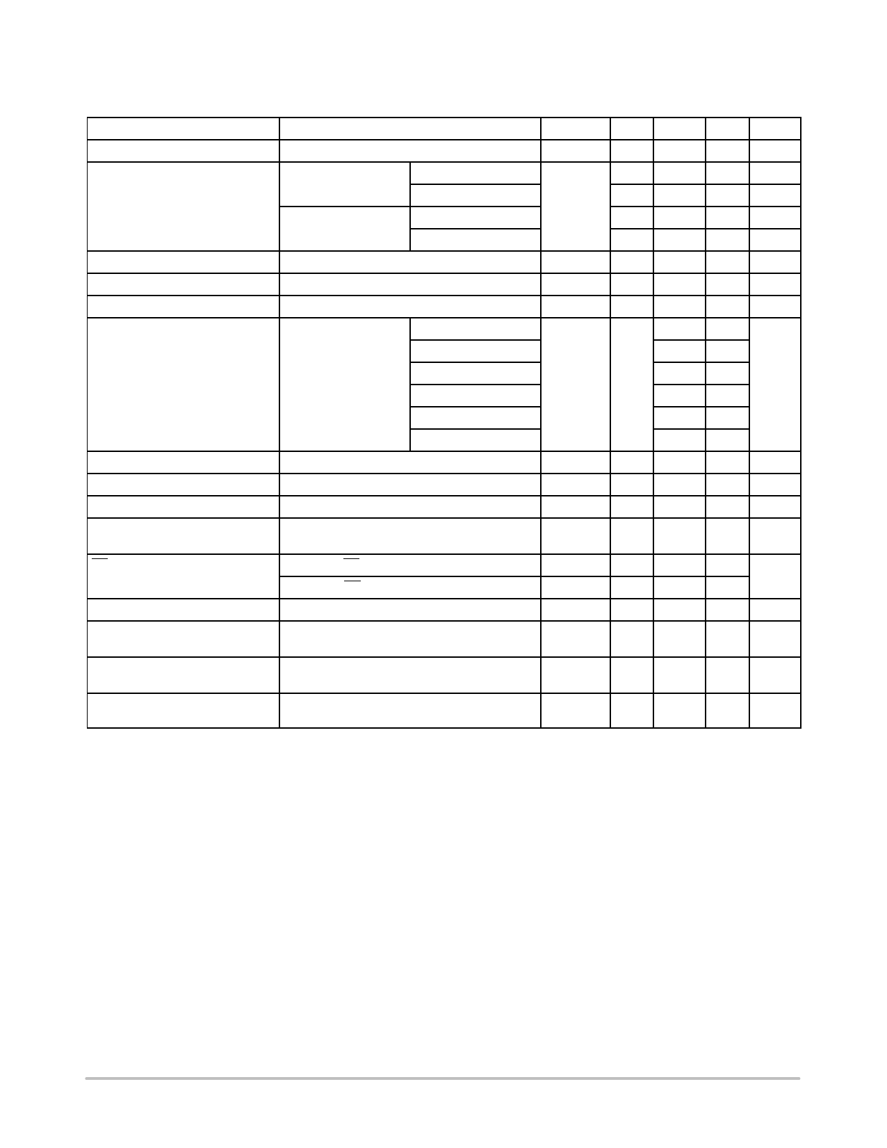
ELECTRICAL CHARACTERISTICS −40°C ≤ TA ≤ 85°C; VIN = VOUT(NOM) + 1 V or 2.5 V, whichever is greater; IOUT = 1 mA, CIN =
COUT = 0.47 mF, unless otherwise noted. Typical values are at TA = +25 °C.
Parameter
Test Conditions
Symbol Min Typ Max Unit
Operating Input Voltage
VIN
1.7
6.5
V
Output Voltage
Output Voltage Temp. Coefficient
Line Regulation
Load Regulation
Dropout Voltage
Output Current
TA = +25 °C
−40°C ≤ TA ≤ 85°C
VOUT > 2 V
VOUT ≤ 2 V
VOUT > 2 V
VOUT ≤ 2 V
TA = −40 to 85°C
VIN = VOUT + 0.5 V to 5 V
IOUT = 1 mA to 150 mA
IOUT = 150 mA
1.2 V ≤ VOUT < 1.5 V
1.5 V ≤ VOUT < 1.7 V
1.7 V ≤ VOUT < 2.0 V
2.0 V ≤ VOUT < 2.5 V
2.5 V ≤ VOUT < 4.0 V
4.0 V ≤ VOUT
VOUT
LineReg
LoadReg
VDO
IOUT
x0.99
−20
x0.985
−30
150
±20
0.02
10
0.67
0.54
0.46
0.41
0.32
0.24
x1.01 V
20
mV
x1.015 V
30
mV
ppm/°C
0.10 %/V
30
mV
1.00
V
0.81
0.68
0.60
0.51
0.37
mA
Short Current Limit
Quiescent Current
VOUT = 0 V
IOUT = 0 mA
ISC
40
mA
IQ
38
58
mA
Standby Current
CE/CE Pin Threshold Voltage
VCE = VIN (L version), VCE = 0 V(H and
D version), TA = 25°C
CE / CE Input Voltage “H”
ISTB
0.1
1
mA
VCEH
1.0
V
CE / CE Input Voltage “L”
VCEL
0.4
CE Pull Down Current
H and D version
IPD
0.4
mA
Power Supply Rejection Ratio
VIN = VOUT + 1 V or 3.0 V whichever is higher,
PSRR
80
dB
IOUT = 30 mA, f = 1 kHz
Output Noise Voltage
VOUT = 1.2 V, IOUT = 30 mA, f = 10 Hz to
VN
100 kHz
30
mVrms
Low Output N−ch Tr. On
Resistance
D Version only, VIN = 4 V, VCE = 0 V
RLOW
30
W
http://onsemi.com
4
Share Link: 