CRCW20101K60JNEF 데이터 시트보기 (PDF) - Vishay Semiconductors
부품명
상세내역
제조사
CRCW20101K60JNEF Datasheet PDF : 10 Pages
| |||
www.vishay.com
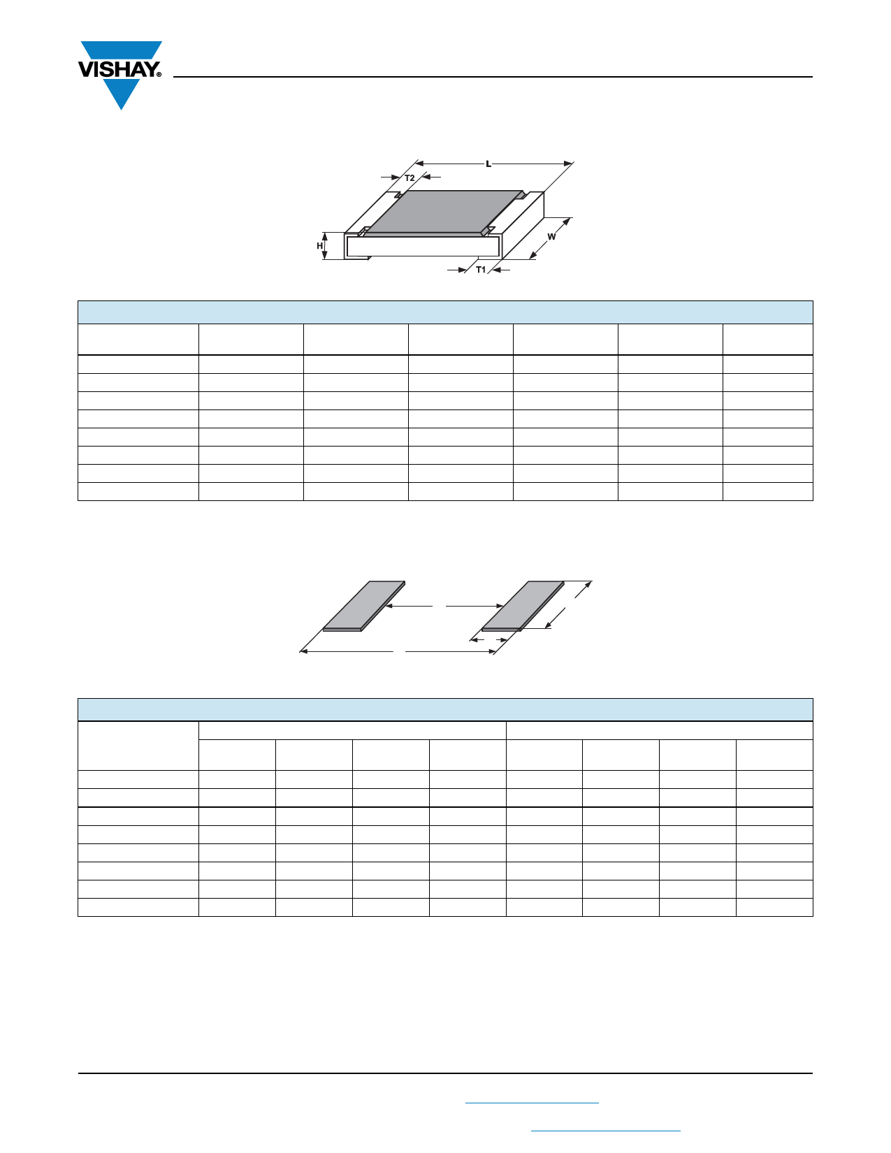
DIMENSIONS
D/CRCW e3
Vishay
DIMENSIONS AND MASS
TYPE / SIZE
L
(mm)
D10/CRCW0402 e3
1.0 ± 0.05
D11/CRCW0603 e3 1.55 + 0.10 / - 0.05
D12/CRCW0805 e3 2.0 + 0.20 / - 0.10
D25/CRCW1206 e3 3.2 + 0.10 / - 0.20
CRCW1210 e3
3.2 ± 0.20
CRCW1218 e3
3.2 + 0.10 / - 0.20
CRCW2010 e3
5.0 ± 0.15
CRCW2512 e3
6.3 ± 0.20
W
(mm)
0.5 ± 0.05
0.85 ± 0.10
1.25 ± 0.15
1.6 ± 0.15
2.5 ± 0.20
4.6 ± 0.15
2.5 ± 0.15
3.15 ± 0.15
SOLDER PAD DIMENSIONS
H
(mm)
0.35 ± 0.05
0.45 ± 0.05
0.45 ± 0.05
0.55 ± 0.05
0.55 ± 0.05
0.55 ± 0.05
0.6 ± 0.10
0.6 ± 0.10
T1
(mm)
0.25 ± 0.05
0.3 ± 0.20
0.3 + 0.20 / - 0.10
0.45 ± 0.20
0.45 ± 0.20
0.45 ± 0.20
0.6 ± 0.20
0.6 ± 0.20
T2
(mm)
0.2 ± 0.10
0.3 ± 0.20
0.3 ± 0.20
0.4 ± 0.20
0.4 ± 0.20
0.4 ± 0.20
0.6 ± 0.20
0.6 ± 0.20
MASS
(mg)
0.65
2
5.5
10
16
29.5
25.5
40.5
G
X
Y
Z
RECOMMENDED SOLDER PAD DIMENSIONS
TYPE / SIZE
G
(mm)
WAVE SOLDERING
Y
(mm)
X
(mm)
Z
(mm)
G
(mm)
REFLOW SOLDERING
Y
(mm)
X
(mm)
Z
(mm)
D10/CRCW0402 e3
-
-
-
-
0.45
0.6
0.6
1.65
D11/CRCW0603 e3
0.65
1.10
1.25
2.85
0.75
0.75
1.00
2.15
D12/CRCW0805 e3
0.90
1.30
1.60
3.50
1.00
0.95
1.45
2.90
D25/CRCW1206 e3
1.40
1.40
1.95
4.20
1.50
1.05
1.80
3.60
CRCW1210 e3
1.80
1.45
2.95
4.70
1.70
1.10
2.80
4.90
CRCW1218 e3
1.80
1.30
5.10
4.40
1.90
1.10
4.90
4.10
CRCW2010 e3
3.40
1.65
2.85
6.90
3.50
1.45
2.80
6.30
CRCW2512 e3
4.60
1.60
3.65
8.70
4.75
1.45
3.50
7.65
Note
• The rated dissipation applies only if the permitted film temperature is not exceeded. Furthermore, a high level of ambient temperature or of
power dissipation may raise the temperature of the solder joint, hence special solder alloys or board materials may be required to maintain
the reliability of the assembly.
The given solder pad dimensions reflect the considerations for board design and assembly as outlined e.g. in standards IEC 61188-5-x or
in publication IPC-7351. They do not guarantee any supposed thermal properties, particularly as these are also strongly influenced by many
other parameters. Still, the given solder pad dimensions will be found adequate for most general applications
Revision: 18-Jun-2018
9
Document Number: 20035
For technical questions, contact: thickfilmchip@vishay.com
THIS DOCUMENT IS SUBJECT TO CHANGE WITHOUT NOTICE. THE PRODUCTS DESCRIBED HEREIN AND THIS DOCUMENT
ARE SUBJECT TO SPECIFIC DISCLAIMERS, SET FORTH AT www.vishay.com/doc?91000
Share Link: 