CAT1163 데이터 시트보기 (PDF) - ON Semiconductor
부품명
상세내역
제조사
CAT1163 Datasheet PDF : 12 Pages
| |||
CAT1163
SPECIFICATIONS
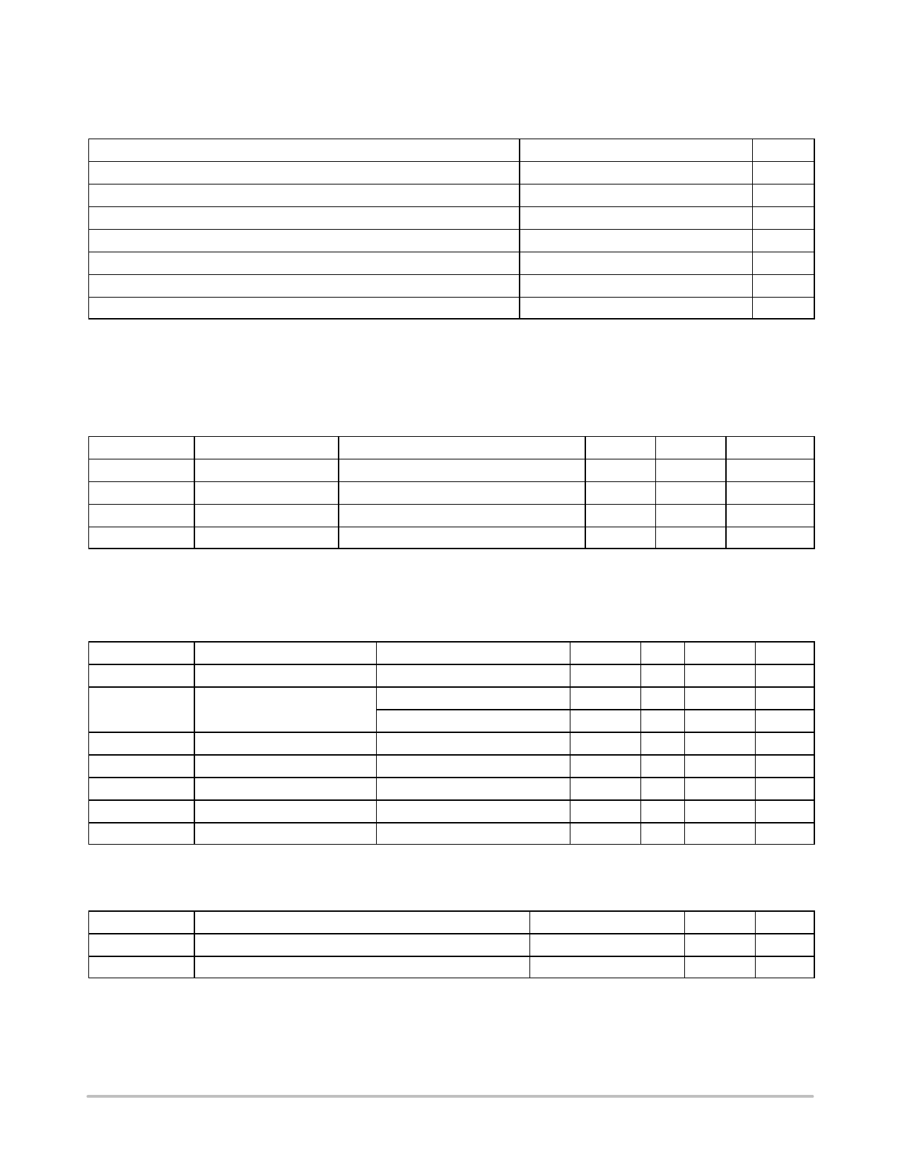
Table 2. ABSOLUTE MAXIMUM RATINGS
Parameters
Ratings
Units
Temperature Under Bias
–55 to +125
°C
Storage Temperature
–65 to +150
°C
Voltage on any Pin with Respect to Ground (Note 1)
VCC with Respect to Ground
Package Power Dissipation Capability (TA = 25°C)
Lead Soldering Temperature (10 seconds)
−2.0 to VCC + 2.0
V
−2.0 to 7.0
V
1.0
W
300
°C
Output Short Circuit Current (Note 2)
100
mA
Stresses exceeding Maximum Ratings may damage the device. Maximum Ratings are stress ratings only. Functional operation above the
Recommended Operating Conditions is not implied. Extended exposure to stresses above the Recommended Operating Conditions may affect
device reliability.
1. The minimum DC input voltage is –0.5 V. During transitions, inputs may undershoot to –2.0 V for periods of less than 20 ns. Maximum
DC voltage on output pins is VCC +0.5 V, which may overshoot to VCC +2.0 V for periods of less than 20 ns.
2. Output shorted for no more than one second. No more than one output shorted at a time.
Table 3. RELIABILITY CHARACTERISTICS
Symbol
Parameter
Reference Test Method
Min
Max
NEND (Note 3) Endurance
MIL−STD−883, Test Method 1033
1,000,000
TDR (Note 3) Data Retention
MIL−STD−883, Test Method 1008
100
VZAP (Note 3) ESD Susceptibility
MIL−STD−883, Test Method 3015
2000
ILTH (Notes 3 & 4) Latch−Up
JEDEC Standard 17
100
3. This parameter is tested initially and after a design or process change that affects the parameter.
4. Latch−up protection is provided for stresses up to 100 mA on address and data pins from –1 V to VCC +1 V.
Units
Cycles/Byte
Years
Volts
mA
Table 4. D.C. OPERATING CHARACTERISTICS
VCC = 2.7 V to 6.0 V, unless otherwise specified.
Symbol
Parameter
Test Conditions
ICC
ISB
ILI
ILO
VIL
VIH
VOL1
Power Supply Current
Standby Current
Input Leakage Current
Output Leakage Current
Input Low Voltage
Input High Voltage
Output Low Voltage (SDA)
fSCL = 100 kHz
VCC = 3.3 V
VCC = 5 V
VIN = GND or VCC
VIN = GND or VCC
IOL = 3 mA, VCC = 3.0 V
Min
−1
VCC x 0.7
Typ
Max
3
40
50
2
10
VCC x 0.3
VCC + 0.5
0.4
Units
mA
mA
mA
mA
mA
V
V
V
Table 5. CAPACITANCE
TA = 25°C, f = 1.0 MHz, VCC = 5 V
Symbol
Test
CI/O (Note 3)
CIN (Note 3)
Input/Output Capacitance (SDA)
Input Capacitance (SCL)
Test Conditions
VI/O = 0 V
VIN = 0 V
Max
Units
8
pF
6
pF
http://onsemi.com
3
Share Link: 