BFQ136 데이터 시트보기 (PDF) - Philips Electronics
부품명
상세내역
제조사
BFQ136 Datasheet PDF : 9 Pages
| |||
Philips Semiconductors
NPN 4 GHz wideband transistor
Product specification
BFQ136
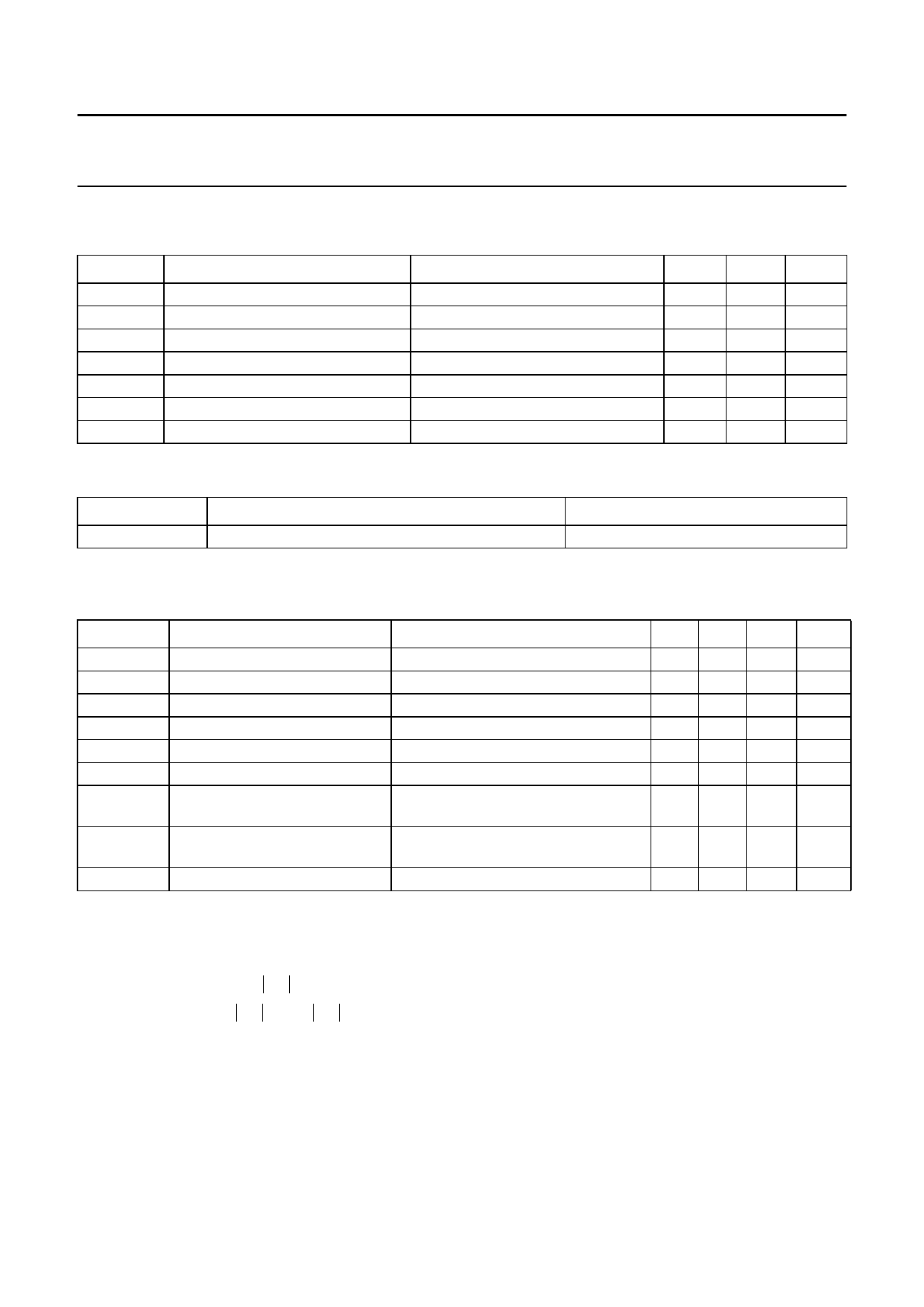
LIMITING VALUES
In accordance with the Absolute Maximum System (IEC 134).
SYMBOL
PARAMETER
CONDITIONS
VCBO
VCEO
VEBO
IC
Ptot
Tstg
Tj
collector-base voltage
collector-emitter voltage
emitter-base voltage
DC collector current
total power dissipation
storage temperature
junction temperature
open emitter
open base
open collector
up to Tc = 100 °C
MIN.
−
−
−
−
−
−65
−
MAX. UNIT
25
V
18
V
2
V
600 mA
9
W
150 °C
200 °C
THERMAL RESISTANCE
SYMBOL
Rth j-c
PARAMETER
thermal resistance from junction to case
THERMAL RESISTANCE
11 K/W
CHARACTERISTICS
Tj = 25 °C unless otherwise specified.
SYMBOL
PARAMETER
CONDITIONS
ICBO
hFE
Cc
Ce
Cre
Ccs
fT
GUM
Vo
collector cut-off current
DC current gain
collector capacitance
emitter capacitance
feedback capacitance
collector-stud capacitance
transition frequency
maximum unilateral power gain
(note 2)
output voltage (see Fig.2)
IE = 0; VCB = 15 V
IC = 500 mA; VCE = 15 V
IE = ie = 0; VCB = 15 V; f = 1 MHz
IC = ic = 0; VEB = 0.5 V; f = 1 MHz
IC = 0; VCE = 15 V; f = 1 MHz
note 1
IC = 500 mA; VCE = 15 V;
f = 500 MHz
IC = 500 mA; VCE = 15 V;
f = 800 MHz; Tamb = 25 °C
note 3
Notes
1. Measured with emitter and base grounded.
2. GUM is the maximum unilateral power gain, assuming S12 is zero and
GUM = 10 log ----1-----–------S----1---1----2S----2---1---1-2----–------S----2--2-----2---- dB.
3. dim = −60 dB; IC = 500 mA; VCE = 15 V; RL = 75 Ω; Tamb = 25 °C;
Vp = Vo at dim = −60 dB; fp = 795.25 MHz;
Vq = Vo −6 dB; fq = 803.25 MHz;
Vr = Vo −6 dB; fr = 805.25 MHz;
measured at f(p+q−r) = 793.25 MHz.
MIN. TYP. MAX. UNIT
−
−
75 µA
25 75 −
−
7.0 −
pF
−
40 −
pF
−
4.0 −
pF
−
0.8 −
−
4.0 −
pF
GHz
−
12.5 −
dB
−
2.5 −
V
September 1995
3
Share Link: 