MHW720A2 데이터 시트보기 (PDF) - Motorola => Freescale
부품명
상세내역
제조사
MHW720A2 Datasheet PDF : 4 Pages
| |||
APPLICATIONS INFORMATION
Nominal Operation
All electrical specifications are based on the nominal
conditions of Vs1 (Pin 5) and Vs2 (Pin 3) equal to 12.5 Vdc
and with output power equaling 20 watts. With these condi-
tions, maximum current density on any device is 1.5 x 10⁵
A/cm2 and maximum die temperature with 100° base plate
temperature is 165°. While the modules are designed to
have excess gain margin with ruggedness, operation of
these units outside the limits of published specifications is
not recommended unless prior communications regarding in-
tended use has been made with the factory representative.
Gain Control
This module is designed for wide range Pout level control.
The recommended method of power output control, as
shown in Figure 3, is to fix Vs1 and Vs2 at 12.5 Vdc and vary
the input RF drive level at Pin 7.
In all applications, the module output power should be lim-
ited to 20 watts.
Decoupling
Due to the high gain of the three stages and the module
size limitation, the external decoupling network requires
careful consideration. Both Pins 3 and 5 are internally by-
passed with a 0.018 µF chip capacitor effective for frequen-
cies from 5 through 470 MHz. For bypassing frequencies
below 5 MHz, networks equivalent to that shown in the test
fixture schematic are recommended. Inadequate decoupling
will result in spurious outputs at certain operating frequen-
cies and certain phase angles of input and output VSWR less
than 4:1.
Load Mismatch
During final test, each module is load mismatch tested in a
fixture having the identical decoupling network described in
Figure 1. Electrical conditions are Vs1 and Vs2 equal 15.5 V,
load VSWR infinite, and output power equal to 30 watts.
Mounting Considerations
To insure optimum heat transfer from the flange to heat-
sink, use standard 6–32 mounting screws and an adequate
quantity of silicon thermal compound (e.g., Dow Corning
340). With both mounting screws finger tight, alternately
torque down the screws to 4–6 inch pounds. The heatsink
mounting surface directly beneath the module flange should
be flat to within 0.005 inch to prevent fracturing of ceramic
substrate material. For more information on module mount-
ing, see EB–107.
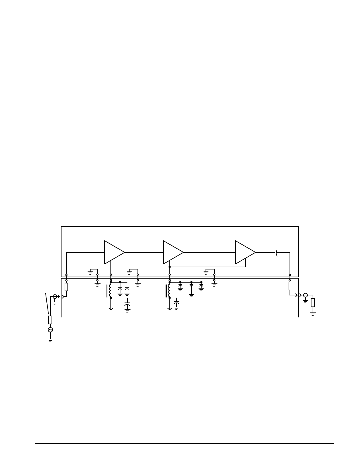
MHW720A BLOCK DIAGRAM
Pin 7
Pin 6 Pin 5
Pin 4
Pin 3
Pin 2
Pin 1
Z1
10 dB
L1 C1
C2
L2
C3 C6 C7
Z2
50
C5
C4
Ohm
Load
Vs1
Vs2
MHW720A Text Fixture Schematic
MICROLAB/ FXR AD 10N
Signal
Generator
Z1, Z2 50 Ω Microstripline
L1, L2 Ferroxcube VK200–20/4B
C1, C4, C5, C6 1.0 µF Tantalum 25 V
C2, C3 0.1 µF Ceramic
C7 47 µF Tantalum, 25 V
NOTE: No Internal D.C. blocking on input pin.
Figure 1. UHF Power Amplifier Test Setup
MHW720A1 MHW720A2
2
MOTOROLA RF DEVICE DATA
Share Link: 