MJD2955(2011) 데이터 시트보기 (PDF) - ON Semiconductor
부품명
상세내역
제조사
MJD2955 Datasheet PDF : 6 Pages
| |||
MJD2955 (PNP)
MJD3055 (NPN)
Complementary Power
Transistors
DPAK For Surface Mount Applications
Designed for general purpose amplifier and low speed switching
applications.
Features
• Lead Formed for Surface Mount Applications in Plastic Sleeves
(No Suffix)
• Straight Lead Version in Plastic Sleeves (“−1” Suffix)
• Electrically Similar to MJE2955 and MJE3055
• DC Current Gain Specified to 10 Amperes
• High Current Gain−Bandwidth Product − fT = 2.0 MHz (Min) @ IC
= 500 mAdc
• Epoxy Meets UL 94 V−0 @ 0.125 in
• ESD Ratings: Human Body Model, 3B u 8000 V
Machine Model, C u 400 V
• These are Pb−Free Packages
MAXIMUM RATINGS
Rating
Collector−Emitter Voltage
Collector−Base Voltage
Emitter−Base Voltage
Collector Current
Base Current
Total Power Dissipation @ TC = 25°C
Derate above 25°C
Total Power Dissipation (Note1)
@ TA = 25°C
Derate above 25°C
Operating and Storage Junction
Temperature Range
Symbol
Max
Unit
VCEO
VCB
VEB
IC
IB
PD{
60
Vdc
70
Vdc
5
Vdc
10
Adc
6
Adc
20
W
0.16
W/°C
PD
W
1.75
0.014 W/°C
TJ, Tstg −55 to +150 °C
THERMAL CHARACTERISTICS
Characteristic
Symbol
Max
Unit
Thermal Resistance, Junction−to−Case
RqJC
6.25
°C/W
Thermal Resistance, Junction−to−Ambient
(Note1)
RqJA
71.4
°C/W
Stresses exceeding Maximum Ratings may damage the device. Maximum
Ratings are stress ratings only. Functional operation above the Recommended
Operating Conditions is not implied. Extended exposure to stresses above the
Recommended Operating Conditions may affect device reliability.
†Safe Area Curves are indicated by Figure 1. Both limits are applicable and must
be observed.
1. These ratings are applicable when surface mounted on the minimum pad
sizes recommended.
http://onsemi.com
SILICON
POWER TRANSISTORS
10 AMPERES
60 VOLTS, 20 WATTS
12
3
4
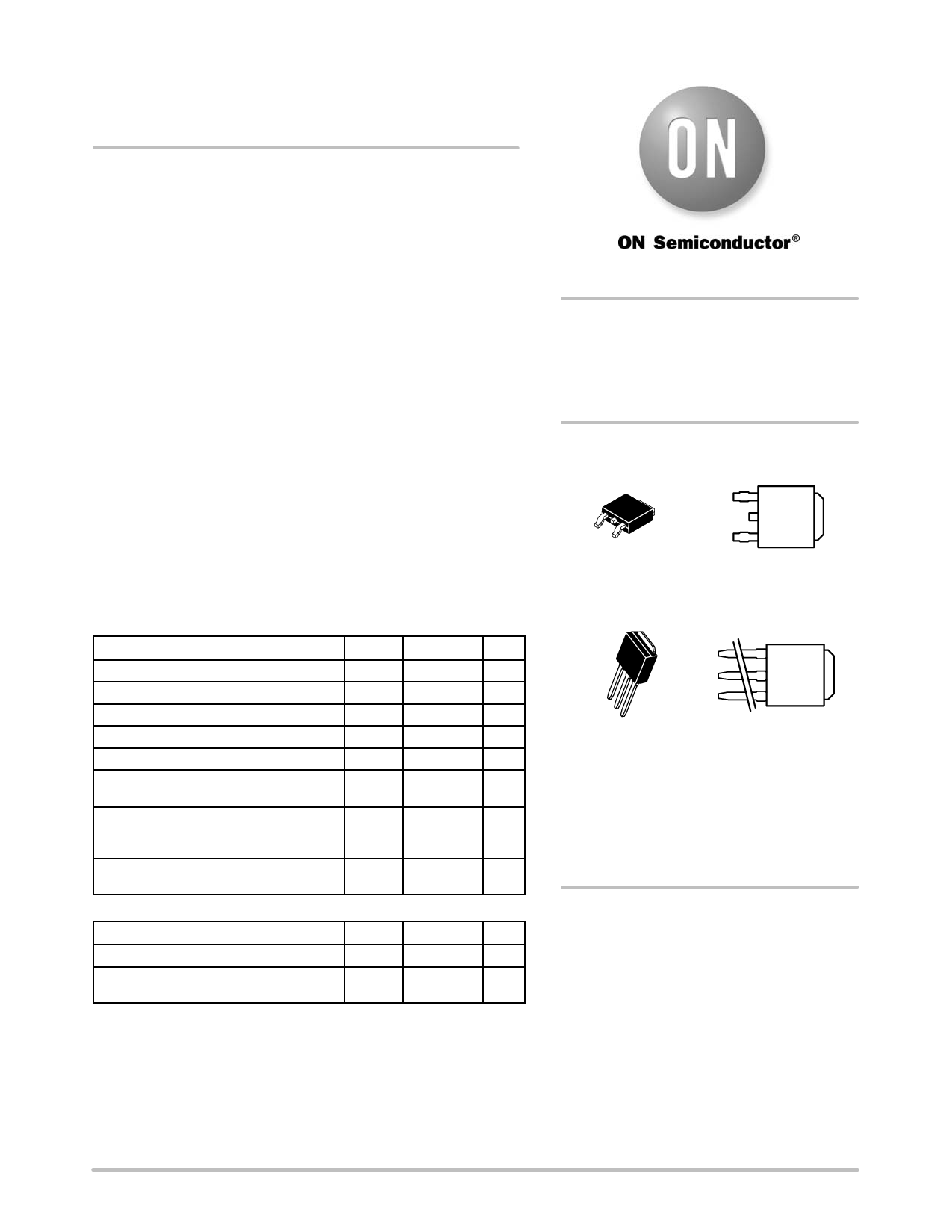
DPAK
CASE 369C
STYLE 1
MARKING
DIAGRAMS
AYWW
J
xx55G
4
1
2
3
DPAK−3
CASE 369D
STYLE 1
AYWW
J
xx55G
A
= Assembly Location
Y
= Year
WW = Work Week
Jxx55 = Device Code
x = 29 or 30
G = Pb−Free Package
ORDERING INFORMATION
See detailed ordering and shipping information in the package
dimensions section on page 2 of this data sheet.
© Semiconductor Components Industries, LLC, 2011
1
January, 2011 − Rev. 10
Publication Order Number:
MJD2955/D
Share Link: 