MX25L1605 데이터 시트보기 (PDF) - Macronix International
부품명
상세내역
제조사
MX25L1605 Datasheet PDF : 45 Pages
| |||
MX25L1605
GENERAL DESCRIPTION
The MX25L1605 is a CMOS 16,777,216 bit serial
eLiteFlashTM Memory, which is configured as 2,097,152 x
8 internally. The MX25L1605 features a serial peripheral
interface and software protocol allowing operation on a
simple 3- wire bus. The three bus signals are a clock input
(SCLK), a serial data input (SI), and a serial data output
(SO). SPI access to the device is enabled by CS# input.
The MX25L1605 provide sequential read operation on
whole chip. User may start to read from any byte of the
array. While the end of the array is reached, the device will
wrap around to the beginning of the array and continuously
outputs data until CS# goes high.
After program/erase command is issued, auto program/
erase algorithms which program/erase and verify the
specified page locations will be executed. Program com-
mand is executed on a page (256 bytes) basis, and erase
command is executed on both chip and sector (64K bytes)
basis.
To provide user with ease of interface, a status register is
included to indicate the status of the chip. The status read
command can be issued to detect completion and error
flag status of a program or erase operation.
To increase user's factory throughputs, a parallel mode is
provided. The performance of read/program is dramatically
improved than serial mode on programmer machine.
When the device is not in operation and CS# is high, it is
put in standby mode and draws less than 50uA DC current.
The additional 4Kb sector with 100K erase/program endur-
ance cycles is suitable for parameter storage and replaces
the EEPROM on system.
The MX25L1605 utilizes MXIC's proprietary memory cell
which reliably stores memory contents even after 10K
program and erase cycles.
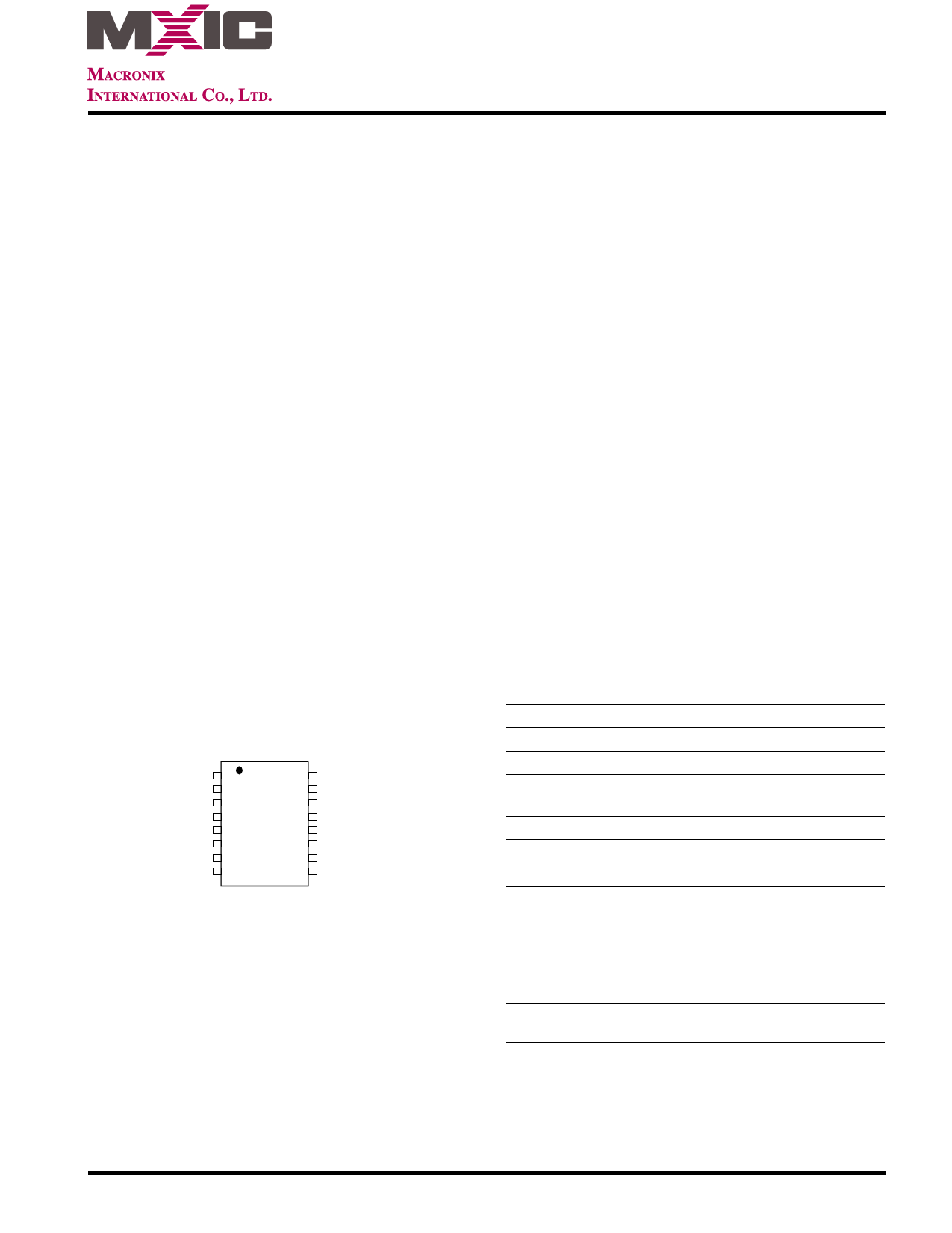
PIN CONFIGURATIONS
16-PIN SOP (300 mil)
HOLD# 1
VCC 2
NC 3
PO2 4
PO1 5
PO0 6
CS# 7
SO/PO7 8
16 SCLK
15 SI
14 PO6
13 PO5
12 PO4
11 PO3
10 GND
9 WP#/ACC
P/N: PM1168
PIN DESCRIPTION
SYMBOL DESCRIPTION
CS#
Chip Select
SI
Serial Data Input
SO/PO7(1) Serial Data Output or Parallel Data
output/input
SCLK
Clock Input
HOLD#(2) Hold, to pause the serial communication
(HOLD# is not for parallel mode)
WP#/ACC Write Protection: connect to GND;
12V for program/erase acceleration:
connect to 12V
VCC
+ 3.3V Power Supply
GND
Ground
PO0~PO6 Parallel data output/input (PO0~PO6 can
be connected to NC in serial mode)
NC
No Internal Connection
Note:
HOLD# is recommended to connect to VCC during parallel
mode.
REV. 1.3, NOV. 06, 2006
2
Share Link: 