AT24C08D 데이터 시트보기 (PDF) - Atmel Corporation
부품명
상세내역
제조사
AT24C08D Datasheet PDF : 28 Pages
| |||
1. Pin Descriptions and Pinouts
Table 1-1. Pin Descriptions
Pin
Number
1, 2
3
4
5
6
7
8
Pin
Symbol
NC
A2
GND
SDA
SCL
WP
VCC
Pin Name and Functional Description
No Connect: The NC pins are not bonded to a die pad. This pin can be
connected to GND or left floating.
Device Address Input: The A2 pin is used to select the hardware device
address and correspond to the fifth bit of the I2C seven bit slave address.
This pin can be directly connected to VCC or GND, allowing up to two
devices on the same bus.
Refer to Note 1 for behavior of the pin when not connected.
Ground: The ground reference for the power supply. GND should be
connected to the system ground.
Serial Data: The SDA pin is an open-drain bidirectional input/output pin
used to serially transfer data to and from the device.
The SDA pin must be pulled-high using an external pull-up resistor (not to
exceed 10K in value) and may be wire-ORed with any number of other
open-drain or open-collector pins from other devices on the same bus.
Serial Clock: The SCL pin is used to provide a clock to the device and to
control the flow of data to and from the device. Command and input data
present on the SDA pin is always latched in on the rising edge of SCL,
while output data on the SDA pin is clocked out on the falling edge of SCL.
The SCL pin must either be forced high when the serial bus is idle or
pulled-high using an external pull-up resistor.
Write Protect: Connecting the WP pin to GND will ensure normal Write
operations. When the WP pin is connected to VCC, all Write operations to
the memory are inhibited.
Refer to Note 1 for behavior of the pin when not connected.
Device Power Supply: The VCC pin is used to supply the source voltage to
the device. Operations at invalid VCC voltages may produce spurious
results and should not be attempted.
Asserted
State
—
—
—
—
—
High
—
Pin
Type
—
Input
Power
Input/
Output
Input
Input
Power
Note:
1. If the A2 or WP pins are not driven, they are internally pulled down to GND. In order to operate in a wide variety of
application environments, the pull-down mechanism is intentionally designed to be somewhat strong. Once these
pins are biased above the CMOS input buffer’s trip point (~0.5 x VCC), the pull-down mechanism disengages.
Atmel recommends connecting these pins to a known state whenever possible.
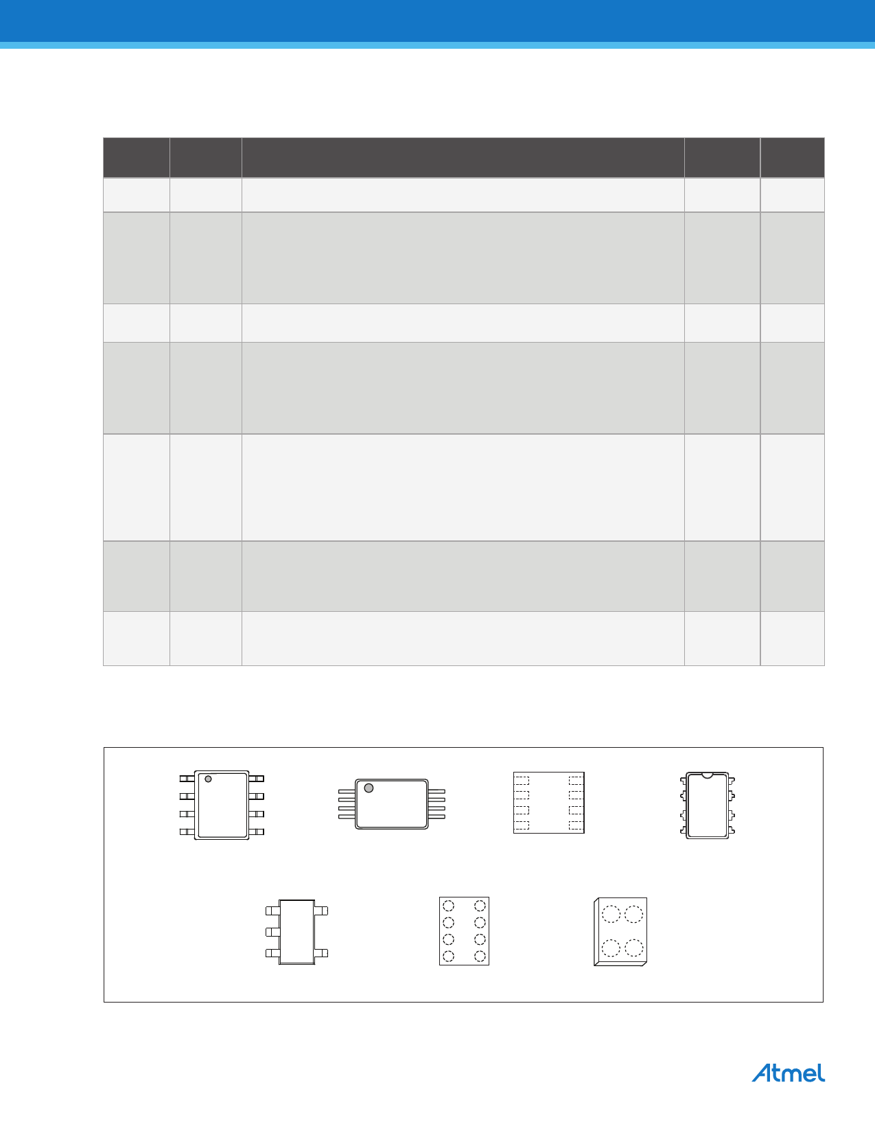
8-lead SOIC
8-lead TSSOP
8-pad UDFN
8-lead PDIP
NC
NC
A2
GND
1
8
2
7
3
6
4
5
Top View
VCC
WP
SCL
SDA
NC
NC
A2
GND
1
8
2
7
3
6
4
5
Top View
VCC
WP
SCL
SDA
NC 1
NC 2
A2 3
GND 4
8 VCC
7 WP
6 SCL
5 SDA
Top View
NC 1
NC 2
A2 3
GND 4
8 VCC
7 WP
6 SCL
5 SDA
Top View
(1)
5-lead SOT23
8-ball VFBGA
(1)
4-ball WLCSP
SCL 1 5 WP
GND 2
SDA
34
VCC
Top View
NC 1
NC 2
A2 3
GND 4
8 VCC
7 WP
6 SCL
5 SDA
Top View
VCC GND
SCL SDA
Top View
Note: Package drawings are not to scale
Note: 1. Refer to “Device Addressing” for details about addressing the SOT23 and WLCSP versions of the device.
2
AT24C08D [DATASHEET]
Atmel-8880B-SEEPROM-AT24C08D-Datasheet_042014
Share Link: 