CXA2095 데이터 시트보기 (PDF) - Sony Semiconductor
부품명
상세내역
제조사
CXA2095 Datasheet PDF : 40 Pages
| |||
Pin
No.
Symbol
41 IREF
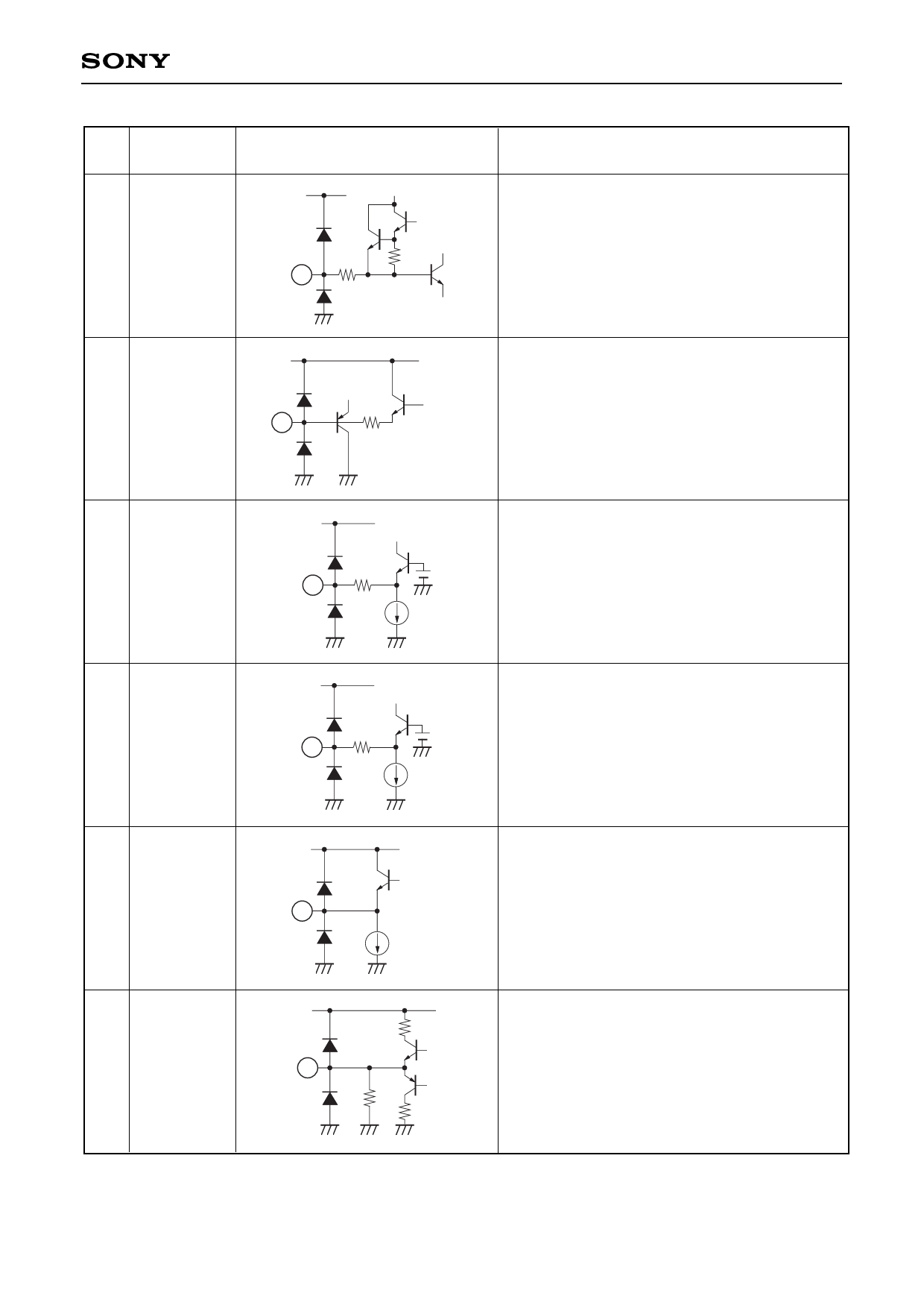
Equivalent circuit
JVCC
147
20k
41
CXA2095S
Description
Internal reference current setting.
Connect to GND via a 15kΩ resistor.
42 VSFIL
JVCC
42
1k
Filter for V sync separation.
Connect to GND via a capacitor.
43 VSIN
44 HSIN
45 VM
46 BGP
JVCC
147
43
20µ
JVCC
147
44
10µ
SVCC
45
400µ
1k
46
15k
1k
Sync signal input for V sync separation.
Input a 2Vp-p Y signal.
Sync signal input for H sync separation.
Input a 2Vp-p Y signal.
Y signal differential waveform output for VM
(Velocity Modulation). (7.1VDC, 2.0Vp-p) The
signal delayed for 250ns from YIN is output.
The delay time from YIN and the differential
coefficient of the output signal vary according to
sharpness f0 control.
Burst gate pulse output.
This pulse is a 0 to 3V positive polarity pulse.
While this pulse is gated near V-Sync for the
CXA2025S, it is constantly output for the
CXA2095S.
–8–
Share Link: 