MC33206 데이터 시트보기 (PDF) - Motorola => Freescale
부품명
상세내역
제조사
MC33206 Datasheet PDF : 12 Pages
| |||
MC33206 MC33207
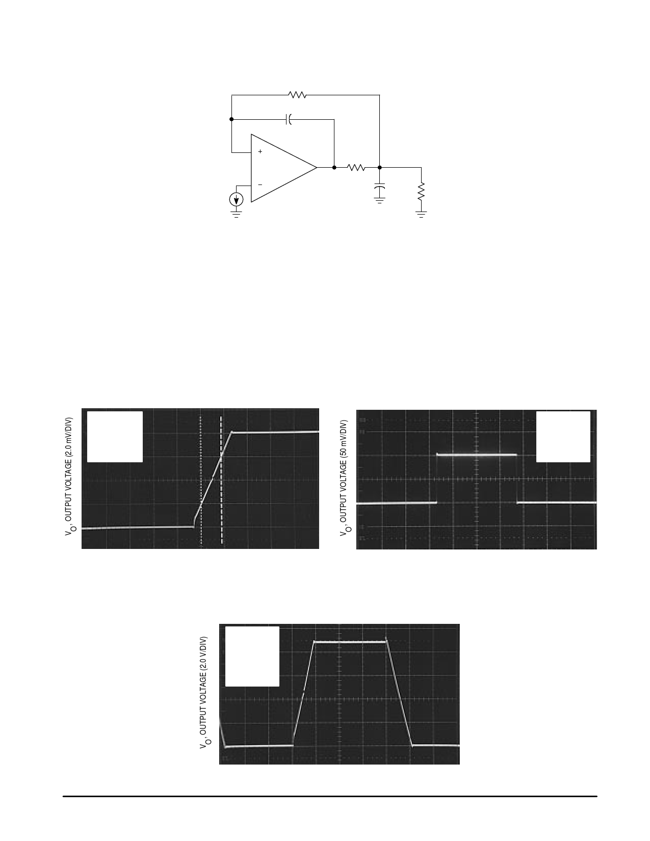
Figure 31. Capacitive Loads Compensation
Rf
CX
RO
Vin
CL
RL
There are several ways to compensate for this
phenomena. Adding series resistance to the output is one
way, but not an ideal solution. A dc voltage error will occur at
the output. A better design solution to compensate for higher
capacitive loads would be to use the circuit in Figure 31. This
design helps to counteract the loss of phase margin by taking
the high frequency output signal and feeding it back into the
amplifier inverting input. This technique helps to overcome
oscillation due to a highly capacitive load. Keep in mind that
compensation will have the affect of lowering the Gain
Bandwidth Product (GPW). The values of CX and R0, are
determined experimentally. Typical CX and CL will be the
same value.
Figure 32. Noninverting Amplifier Slew Rate
VCC = 6.0 V
VEE = –6.0 V
RL = 600 Ω
CL = 100 pF
TA = 25°C
SPICE Model
If a SPICE Macromodel is desired for the MC33206/07,
the user can define the characteristics from the following
information. Obtain the SPICE Macromodel for the MC33204
Rail–to–Rail Operational Amplifier (device is the same as the
MC33207). For the Enable feature of the MC33207, simulate
it as a bipolar switch. The Macromodel does not include an
input capacitance between the inverting and noninverting
inputs. This capacitor is called Cin. Add 3.0 to 5.0 pF if
stability analysis is required.
Figure 33. Small Signal Transient Response
VCC = 6.0 V
VEE = –6.0 V
RL = 600 Ω
CL = 100 pF
TA = 25°C
t, TIME (5.0 µs/DIV)
t, TIME (10 µs/DIV)
Figure 34. Large Signal Transient Response
VCC = 6.0 V
VEE = –6.0 V
RL = 600 Ω
CL = 100 pF
AV = 1.0
TA = 25°C
t, TIME (10 µs/DIV)
10
MOTOROLA ANALOG IC DEVICE DATA
Share Link: 