MC33206 데이터 시트보기 (PDF) - Motorola => Freescale
부품명
상세내역
제조사
MC33206 Datasheet PDF : 12 Pages
| |||
MC33206 MC33207
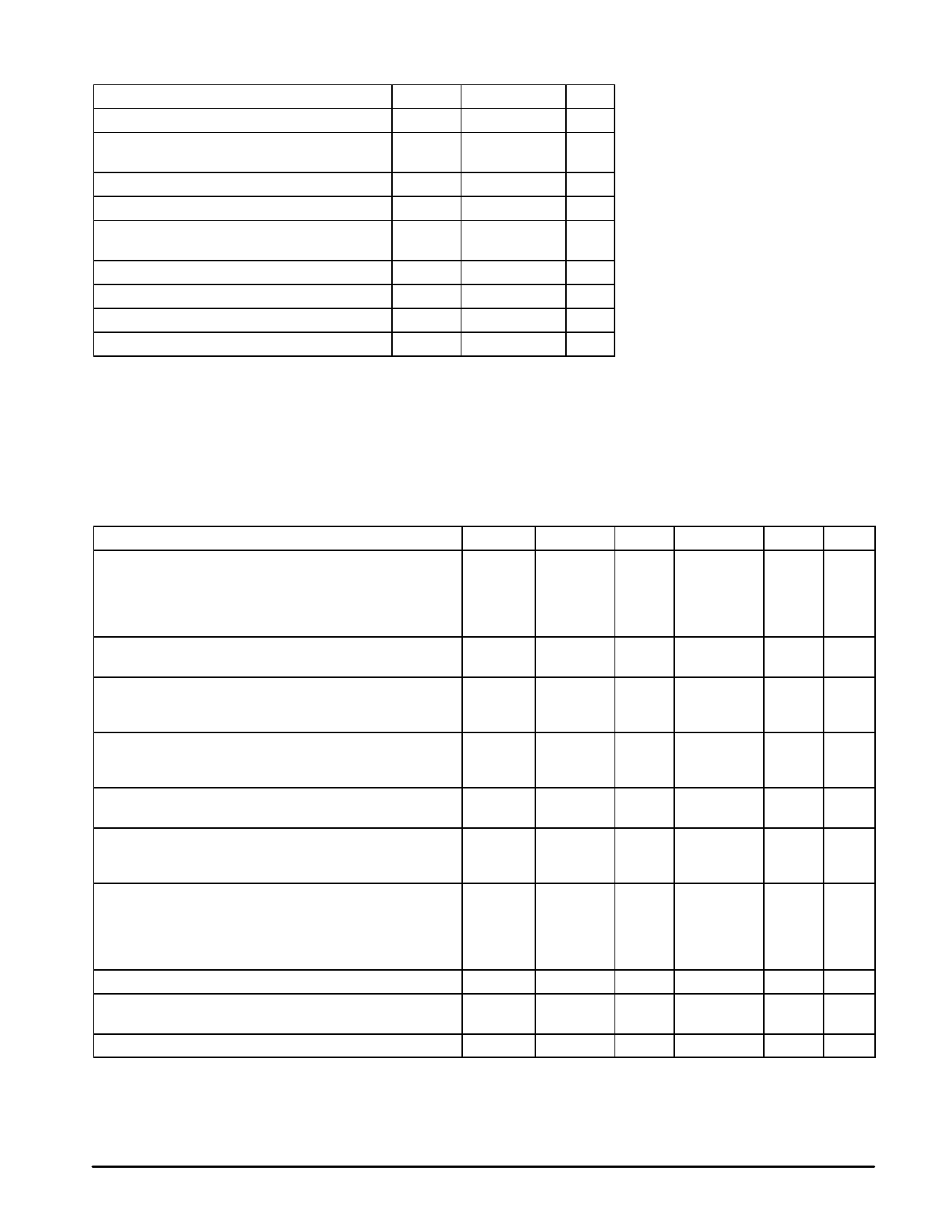
MAXIMUM RATINGS
Rating
Symbol
Value
Unit
Supply Voltage (VCC to VEE)
ESD Protection Voltage at any Pin
Human Body Model
VS
13
V
VESD
2,000
V
Voltage at any Device Pin
Input Differential Voltage Range
Common Mode Input Voltage Range (Note 2)
VDP
VS ± 0.5
V
VIDR
(Note 1)
V
VCM
VCC + 0.5 to
V
VEE – 0.5
Output Short Circuit Duration (Note 3)
ts
(Note 3)
sec
Maximum Junction Temperature
TJ
+150
°C
Storage Temperature Range
Tstg
–65 to +150
°C
Maximum Power Dissipation
PD
(Note 3)
mW
NOTES: 1. The differential input voltage of each amplifier is limited by two internal parallel back–to–back
diodes. For additional differential input voltage range, use current limiting resistors in series
with the input pins.
2. The common–mode input voltage range of each amplifier is limited by diodes connected from
the inputs to both power supply rails. Therefore, the voltage on either input must not exceed
either supply rail by more than 500 mV.
3. Power dissipation must be considered to ensure maximum junction temperature (TJ) is not
exceeded.
4. ESD data available upon request.
DC ELECTRICAL CHARACTERISTICS (VCC = 5.0 V, VEE = 0 V, VEnable = 5.0 V, TA = 25°C, unless otherwise noted.)
Characteristic
Figure
Symbol
Min
Typ
Max
Input Offset Voltage (VCM 0 to 0.5 V, VCM 1.0 to 5.0 V)
MC33206: TA = 25°C
MC33201: TA = –40° to +105°C
MC33207: TA = 25°C
MC33202: TA = –40° to +105°C
–
VIO
–
0.5
8.0
–
1.0
11
–
0.5
10
–
1.0
13
Input Offset Voltage Temperature Coefficient (RS = 50 Ω)
TA = –40° to +105°C
–
∆VIO/∆T
–
2.0
–
Input Bias Current (VCM = 0 to 0.5 V, VCM = 1.0 to 5.0 V)
TA = 25°C
TA = –40° to +105°C
Input Offset Current (VCM = 0 to 0.5 V, VCM = 1.0 to 5.0 V)
TA = 25°C
TA = –40° to +105°C
–
IIB
–
–
–
IIO
–
–
80
200
100
250
5.0
50
10
100
Common Mode Input Voltage Range
–
VICR
–
VCC + 0.2
VCC
VEE
VEE – 0.2
–
Large Signal Voltage Gain (VCC = 5.0 V, VEE = –5.0 V)
RL = 10 kΩ
RL = 600 Ω
–
AVOL
50
300
–
25
250
–
Output Voltage Swing (VID = ±0.2 V)
RL = 10 kΩ
RL = 10 kΩ
RL = 600 Ω
RL = 600 Ω
–
VOH
4.85
4.95
–
VOL
–
0.05
0.15
VOH
4.75
4.85
–
VOL
–
0.15
0.25
Common Mode Rejection (Vin = 0 to 5.0 V)
Power Supply Rejection Ratio
VCC/VEE = 5.0 V/Gnd to 3.0 V/Gnd
–
CMR
60
–
PSRR
–
PSR
66
90
–
25
500
92
–
Output Short Circuit Current (Source and Sink)
–
ISC
50
80
–
Unit
mV
µV/°C
nA
nA
V
kV/V
V
dB
µV/V
dB
mA
2
MOTOROLA ANALOG IC DEVICE DATA
Share Link: 