MC33206 데이터 시트보기 (PDF) - Motorola => Freescale
부품명
상세내역
제조사
MC33206 Datasheet PDF : 12 Pages
| |||
MC33206 MC33207
GENERAL INFORMATION
The MC33206/7 family of operational amplifiers are
unique in their ability to swing rail–to–rail on both the input
and the output with a completely bipolar design. This offers
low noise, high output current capability and a wide common
mode input voltage range even with low supply voltages.
Operation is guaranteed over an extended temperature
range and at supply voltages of 2.0 V, 3.3 V and 5.0 V and
ground.
Since the common mode input voltage range extends from
VCC to VEE, it can be operated with either single or split
voltage supplies. The MC33206/7 are guaranteed not to latch
or phase reverse over the entire common mode range,
however, the inputs should not be allowed to exceed
maximum ratings.
CIRCUIT INFORMATION
Rail–to–rail performance is achieved at the input of the
amplifiers by using parallel NPN–PNP differential input
stages. When the inputs are within 800 mV of the negative
rail, the PNP stage is on. When the inputs are more than
800 mV greater than VEE, the NPN stage is on. This
switching of input pairs will cause a reversal of input bias
currents (see Figure 6). Also, slight differences in offset
voltage may be noted between the NPN and PNP pairs.
Cross–coupling techniques have been used to keep this
change to a minimum.
In addition to its rail–to–rail performance, the output stage
is current boosted to provide 80 mA of output current,
enabling the op amp to drive 600 Ω loads. Because of this
high output current capability, care should be taken not to
exceed the 150°C maximum junction temperature.
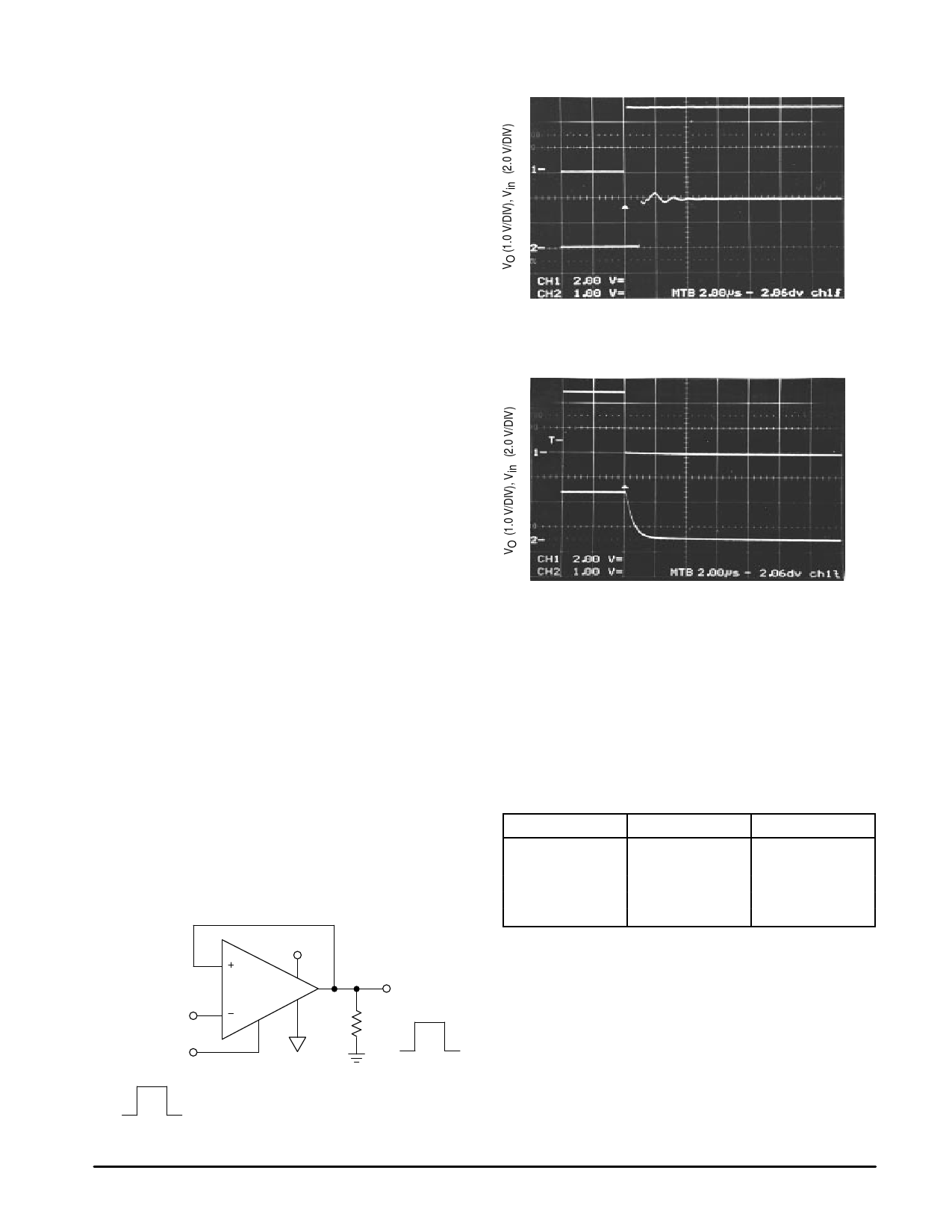
Enable Function
The MC33206/07 enable pins allow the user to externally
control the device. (Refer to the Pin Diagram on the first page
of this data sheet for enable pin connections.) If the enable
pins are pulled low (Gnd) each amplifier (MC33206) and
amplifier pair (MC33207) will be disabled. When the enable
pins are at a logic high (VEnable ≥ VEE = 1.8 V) the amplifiers
will turn “on”. Refer to the data sheet characteristics for the
required levels needed to change logical state.
The time to change states (from device “on” to “off” and
“off” to “on”) is defined as the time delay. The Circuit in
Figure 27 is used to measure ton and toff. Typical ton and toff
measurements are shown in Figures 28 and 29. When the
device is turned off (VEnable = Gnd) an internal regulator is
shut off disabling the amplifier.
Figure 27. Test Circuit for ton and toff
VCC
2.0 V
VEnable
ton toff
MC33206
2.0 k
Vout
ton toff
Figure 28. ton Response
ton, TIME (2.0 µs/DIV)
Figure 29. toff Response
toff, TIME (2.0 µs/DIV)
Low Voltage Operation
The MC33206/07 will operate at supply voltages down to
1.8 V and ground. Since this device is a rail–to–rail on both
the input and output, one can be assured of continued
operation in battery applications when battery voltages drop
to low voltage levels. This is called End of Discharge (see
Figure 30). Now, the user can select a minimum quantity of
batteries best suited for the particular design depending on
the type of battery chosen. This will minimize part count in
many designs.
Figure 30. Typical Battery Characteristics
Type
Alkaline
NiCd
NiMh
Silver Oxide
Lithium Ion
Operating Voltage
1.5 V
1.2 V
1.2 V
1.6 V
3.6 V
End of Discharge
0.9 V
1.0 V
1.0 V
1.3 V
2.5 V
Compensating for Output Capacitance
The combination of device output impedance and
increasing capacitive loading will cause phase delay
(reducing the phase margin) in any amplifier (Figure 22). If
the loading is excessive, the resulting response can be circuit
oscillation. In other words, an amplifier can become unstable
when the phase becomes greater than 180 degrees before
the open loop gain drops to unity gain. Figures 18 and 19
show this situation as frequency increases for a given load.
The MC33206/7 can typically drive up to 300 pF loads at
unity gain without oscillating.
MOTOROLA ANALOG IC DEVICE DATA
9
Share Link: 