RF9908PCBA 데이터 시트보기 (PDF) - RF Micro Devices
부품명
상세내역
제조사
RF9908PCBA Datasheet PDF : 4 Pages
| |||
RF9908
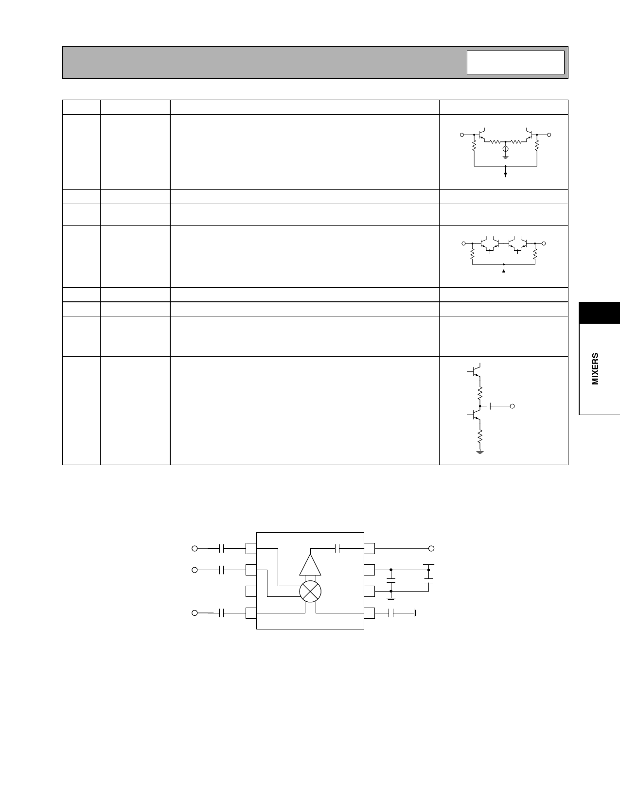
Pin Function Description
Interface Schematic
1
IF+
Balanced IF Input Pin. This pin is internally DC biased and should be
DC blocked if connected to a device with a DC level present. For single-
IF+
IF-
ended input operation, one pin is used as an input and the other IF
input is AC coupled to ground. The balanced, as well as single-ended,
input impedance is 265Ω.
BIAS
2
IF-
Same as pin 1, except complementary input.
See pin 1.
3
GND
Ground connection. Keep traces physically short and connect immedi-
ately to ground plane for best performance.
4
LO+
Balanced LO Input Pin. This pin is internally DC biased and should be
DC blocked if connected to a device with a DC level present. For single- LO+
LO-
ended input operation, one pin is used as an input and the other LO
input is AC coupled to ground. The balanced, as well single-ended,
input impedance is 50Ω.
BIAS
5
LO-
Same as pin 4, except complementary input.
See pin 4.
6
GND
Same as pin 3.
6
7
VCC
Supply Voltage pin. External bypassing is required. External RF, LO,
and IF bypassing is required. The trace length between the pin and the
bypass capacitors should be minimized. The ground side of the bypass
capacitors should connect immediately to ground plane.
8
RF OUT RF Output Pin. This pin is internally DC blocked. The output impedance
is 50Ω.
RF OUT
Application Schematic
IF+
IF-
LO+
1 nF
1
1 nF
2
3
100 pF
4
8
RF OUT
VCC
7
100 pF 100 nF
6
5
100 pF
Rev A2 010720
6-59
Share Link: 