MTW14N50E 데이터 시트보기 (PDF) - ON Semiconductor
부품명
상세내역
제조사
MTW14N50E Datasheet PDF : 8 Pages
| |||
MTW14N50E
Preferred Device
Power MOSFET
14 Amps, 500 Volts
N–Channel TO–247
This high voltage MOSFET uses an advanced termination scheme
to provide enhanced voltage–blocking capability without degrading
performance over time. In addition, this advanced Power MOSFET is
designed to withstand high energy in the avalanche and commutation
modes. The new energy efficient design also offers a drain–to–source
diode with a fast recovery time. Designed for high voltage, high speed
switching applications in power supplies, converters and PWM motor
controls, these devices are particularly well suited for bridge circuits
where diode speed and commutating safe operating areas are critical
and offer additional safety margin against unexpected voltage
transients.
• Robust High Voltage Termination
• Avalanche Energy Specified
• Source–to–Drain Diode Recovery Time Comparable to a Discrete
Fast Recovery Diode
• Diode is Characterized for Use in Bridge Circuits
• IDSS and VDS(on) Specified at Elevated Temperature
• Isolated Mounting Hole Reduces Mounting Hardware
MAXIMUM RATINGS (TC = 25°C unless otherwise noted)
Rating
Symbol Value
Drain–Source Voltage
Drain–Gate Voltage (RGS = 1.0 MΩ)
Gate–Source Voltage – Continuous
Drain Current – Continuous
Drain Current – Continuous @ 100°C
Drain Current – Single Pulse (tp ≤ 10 µs)
Total Power Dissipation
Derate above 25°C
VDSS
500
VDGR
500
VGS
±20
ID
14
ID
9.0
IDM
60
PD
180
1.44
Operating and Storage Temperature Range TJ, Tstg –55 to
150
Single Pulse Drain–to–Source Avalanche
Energy – Starting TJ = 25°C
(VDD = 50 Vdc, VGS = 10 Vpk,
IL = 14 Apk, L = 8.8 mH, RG = 25 Ω )
EAS
860
Thermal Resistance – Junction to Case
RθJC
0.7
Thermal Resistance – Junction to Ambient
RθJA
40
Maximum Lead Temperature for Soldering
TL
260
Purposes, 1/8″ from case for 10 seconds
Unit
Vdc
Vdc
Vdc
Adc
Apk
Watts
W/°C
°C
mJ
°C/W
°C
http://onsemi.com
14 AMPERES
500 VOLTS
RDS(on) = 400 mΩ
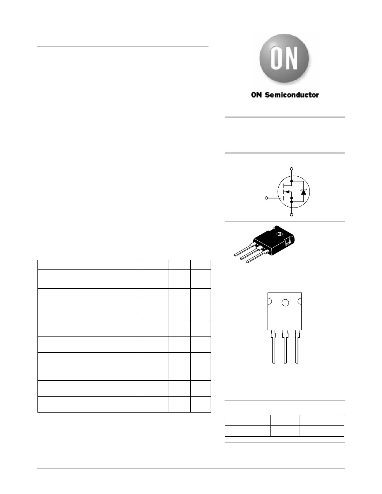
N–Channel
D
G
1
23
S
4
TO–247AE
CASE 340K
Style 1
MARKING DIAGRAM
& PIN ASSIGNMENT
4
Drain
MTW14N50E
LLYWW
1
Gate
3
Source
2
Drain
LL
= Location Code
Y
= Year
WW = Work Week
ORDERING INFORMATION
Device
Package
Shipping
MTW14N50E
TO–247
30 Units/Rail
Preferred devices are recommended choices for future use
and best overall value.
© Semiconductor Components Industries, LLC, 2000
1
November, 2000 – Rev. 5
Publication Order Number:
MTW14N50E/D
Share Link: 