SN7808PI 데이터 시트보기 (PDF) - Kodenshi Auk Co., LTD
부품명
상세내역
제조사
SN7808PI Datasheet PDF : 18 Pages
| |||
SN78xxx
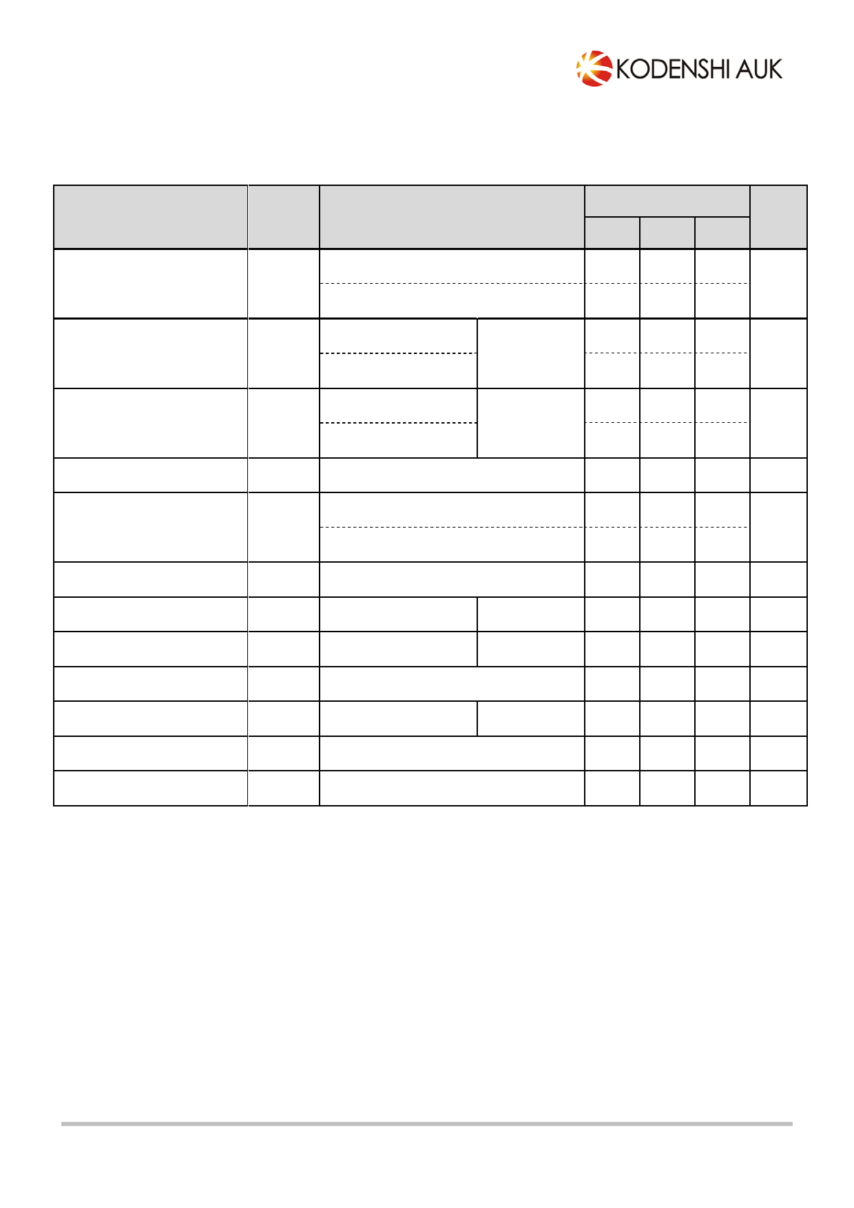
◈ Electrical characteristics
( VIN=19V, CIN = 0.33uF, COUT = 0.1 uF, IOUT = 500mA, TJ=0℃~125℃ ; unless otherwise specified )
Characteristic
Symbol
Test Condition*
SN7812x
Unit
Min. Typ. Max.
Output Voltage**
Line Regulation
TJ =25℃
VO
14.5V ≤ VIN ≤ 27.0V
5.0mA ≤ IO ≤ 1.0A, PD ≤ 15W
ÌVO(△VI)
14.5V ≤ VIN ≤ 30.0V
16.0V ≤ VIN ≤ 22.0V
TJ =25℃
11.50 12.00 12.50
V
11.40 12.00 12.60
-
10.0
240
mV
-
3.0
120
Load Regulation
ÌVO(△IL)
5.0mA ≤ IO ≤ 1.5A
250mA ≤ IO ≤ 750mA
TJ =25℃
-
11.0
240
mV
-
5.0
120
Quiescent Current
IQC
TJ =25℃
-
5.1
8.0
mA
Quiescent Current Change
Ripple Rejection
Dropout Voltage
ÌIQC
RR
VDROP
14.5V ≤ VIN ≤ 30.0V
5.0mA ≤ IO ≤ 1.0A
15.0V ≤ VIN ≤ 25.0V
f=120Hz
IO=1.0A
TJ =25℃
-
0.5
1.0
mA
-
0.1
0.5
55
71
-
dB
-
2.0
-
V
Output Noise Voltage
VN
10Hz ≤ f ≤ 100kHz
TA =25℃
-
76
-
uV/ VO
Output Resistance
rO
f=1.0kHz
-
15
-
mΩ
Short Circuit Current
ISC
VI =35V
TA =25℃
-
250
-
mA
Peak Output Current
IPK
TJ =25℃
-
2.2
-
A
Temperature coefficient of
Output voltage
△VO/
△Temp
IO=5.0mA
-
-1.0
-
mV/°C
* Pulse testing techniques are used to maintain the junction temperature as close to the ambient
temperature as possible. Thermal effects must be taken into separately.
** This specification applies only for dc power dissipation permitted by absolute maximum ratings.
KSD-I0O008-004
9
Jan. 2010 REV. 04
Share Link: 