FA5304AP 데이터 시트보기 (PDF) - Collmer Semiconductor
부품명
상세내역
제조사
FA5304AP Datasheet PDF : 17 Pages
| |||
FA5304AP(S)/FA5305AP(S)
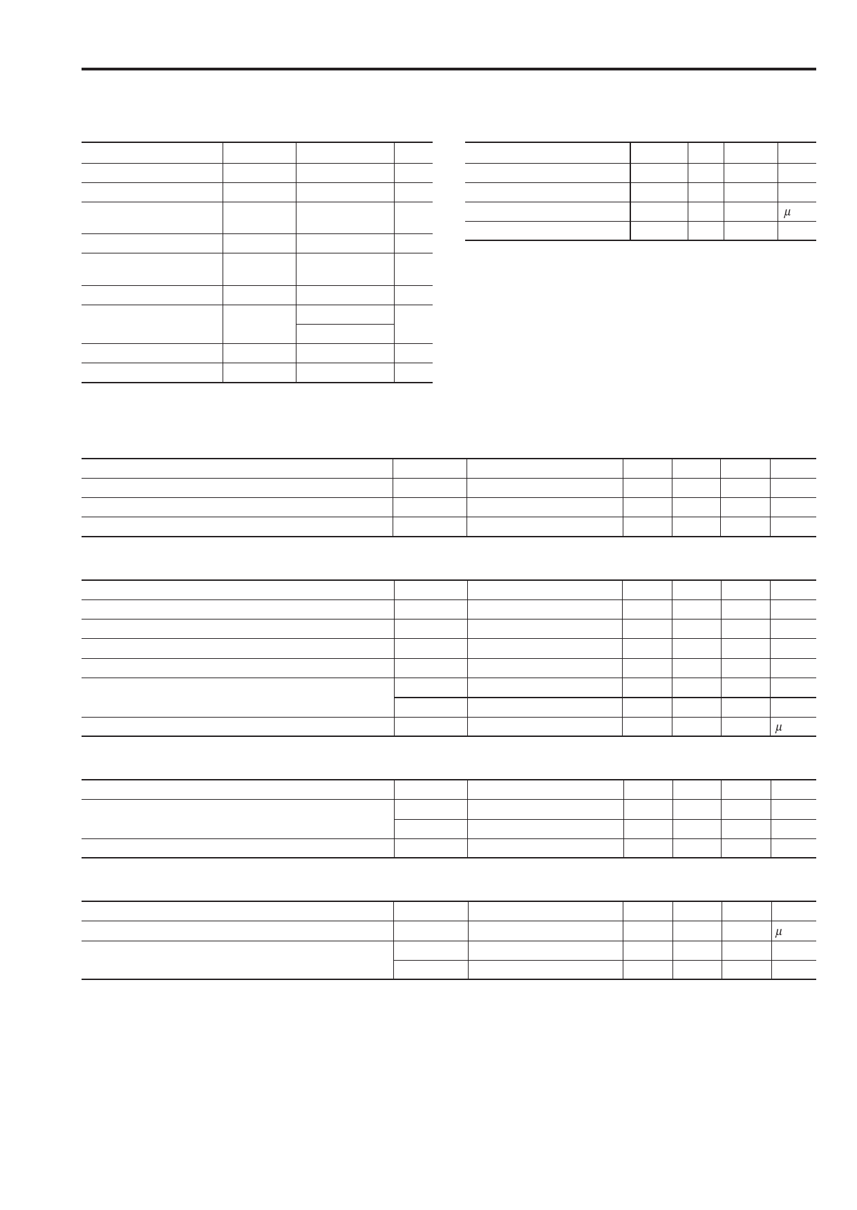
s Absolute maximum ratings
Common to FA5304AP(S) and FA5305AP(S)
Item
Supply voltage
Output current
Error amplifier input
voltage
Feedback terminal input voltage
Overcurrent detection
terminal input voltage
CS terminal input current
Total power dissipation
(Ta = 25°C)
Symbol
VCC
IO
VIN
VFB
VIS
ICS
Pd
Operating temperature
Topr
Storage temperature
Tstg
Rating
Unit
30
V
±1.5
A
4
V
4
V
–0.3 to +4
V
2
mA
800 (DIP-8) *1 mW
550 (SOP-8) *2
–30 to +85
°C
–40 to +150
°C
s Recommended operating conditions
Common to FA5304AP(S) and FA5305AP(S)
Item
Symbol Min. Max. Unit
Supply voltage
VCC
10 30
V
Error amplifier feedback resistor RNF
100
kΩ
Soft-start capacitor
CS
0.1 1
µF
Oscillation frequency
fOSC
5
600
kHz
Notes:
*1 Derating factor Ta > 25°C : 8.0mW/°C ( on PC board )
*2 Derating factor Ta > 25°C : 5.5mW/°C ( on PC board )
s Electrical characteristics (Ta=25°C, VCC=18V,fosc=135kHz)
Oscillator section Common to FA5304AP(S) and FA5305AP(S)
Item
Oscillation frequency
Frequency variation 1 (due to supply voltage change)
Frequency variation 2 (due to temperature change)
Symbol
fOSC
fdv
fdT
Test condition
CT = 360pF
VCC = 10 to 30V
Ta = –30 to +85°C
Min.
112
Typ.
135
±1
±4
Max. Unit
148
kHz
%
%
Error amplifier section Common to FA5304AP(S) and FA5305AP(S))
Item
Reference voltage
Input bias current
Open-loop voltage gain
Unity-gain bandwidth
Maximum output voltage (Pin 2)
Output source current (Pin 2)
Symbol
VB
IB
AV
fT
VOM+
VOM–
IMO+
Test condition
V1 = 2V
RNF = 100kΩ
RNF = 100kΩ
VOM = 1V
Min.
1.90
–500
80
2.70
Typ.
2.00
–50
1.0
–100
Max.
2.10
200
–50
Unit
V
nA
dB
MHz
V
mV
µA
Pulse width modulation circuit section Common to FA5304AP(S) and FA5305AP(S)
Item
Input threshold voltage (Pin 2)
Maximum duty cycle
Symbol
VTH FBO
VTH FBM
DMAX
Test condition
Duty cycle = 0%
Duty cycle = DMAX
Min.
0.80
1.70
42
Typ.
1.00
1.90
45
Max. Unit
1.20 V
2.10 V
50
%
Soft-start circuit section Common to FA5304AP(S) and FA5305AP(S)
Item
Charge current (Pin 8)
Input threshold voltage (Pin 8)
Symbol
ICHG
VTH CSO
VTH CSM
Test condition
Pin 8 = 0V
Duty cycle = 0%
Duty cycle = DMAX
Min. Typ. Max. Unit
–15
–10
–5
µA
0.80 1.00 1.20 V
1.70 1.90 2.10 V
3
Share Link: 