ML7041 데이터 시트보기 (PDF) - Unspecified
부품명
상세내역
제조사
ML7041 Datasheet PDF : 28 Pages
| |||
FEDL7041-05
ML7041
PIN DESCRIPTIONS
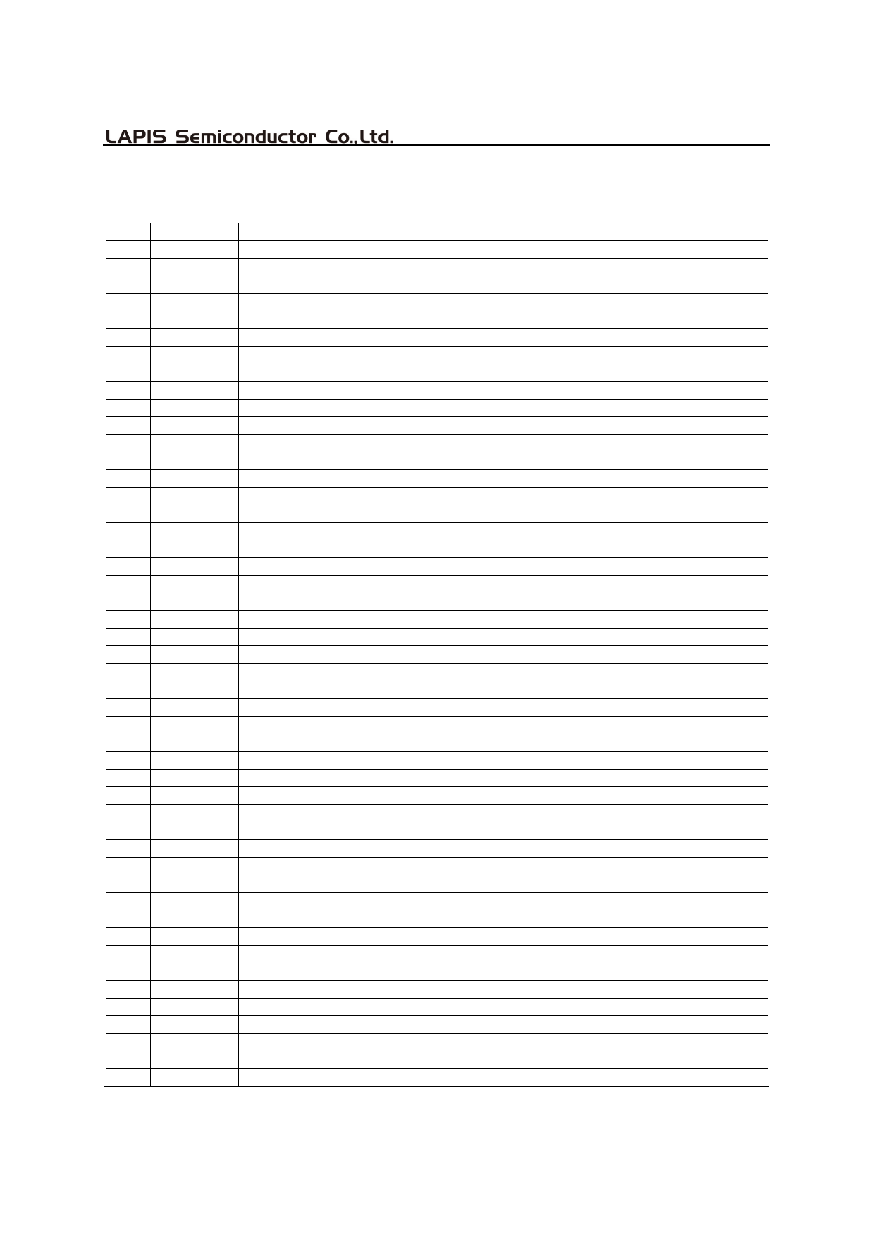
Pin
Symbol Type
Description
1
AG
— Analog ground (0 V)
2
EAR2O
O Receive side voice amplifier output 2
3
EAR1O
O Receive side voice amplifier output 1
4
VA1
— Analog power supply 1 (3.0 V)
5
EXTO
O Receive side voice amplifier output
6
EXTI
I Receive side voice amplifier input
7
VA2
— Analog power supply 2 (3.0 V)
8
SPO–
O Receive side voice amplifier output–
9
AG2
— Analog ground 2 (0 V)
10
AG3
— Analog ground 3 (0 V)
11
SPO+
O Receive side voice amplifier output+
12
VA3
— Analog power supply 3 (3.0 V)
13
AGGP1
— General purpose port ground 1 (0 V)
14
GP1
O General purpose port 1 output (Open drain)
15
GP2
O General purpose port 2 output (Open drain)
16
GP3
O General purpose port 3 output (Open drain)
17
GP4
O General purpose port 4 output (Open drain)
18
AGGP2
— General purpose port ground 2 (0 V)
19
VDD
— Digital power supply (3.0 V)
20
MCK
I Master clock input (2.048 MHz)
21
SDA
I/O I2C data input/output (Pull-up resister required)
22
SCL
I I2C shift clock input
23
PCMIN
I PCM receive signal input
24 PCMOUT O PCM transmit signal output
25
DG
— Digital ground (0 V)
26
BCLK
I PCM data shift clock input
27
SYNC
I PCM data shift sync signal input
28
PDN
I Power down control input
29 RG1PDN
I Power down input for regulator 1 (3.0 V/0 V)
30 RG2PDN
I Power down input for regulator 2 (3.0 V/0 V)
31
AGR1
— Ground for regulator 1 (0 V)
32
RG1O
O Regulator 1 output (3.0 V)
33
RG1IN
I Regulator 1 power input (3.6 V)
34
AGR2
— Ground for regulator 2 (0 V)
35
RG2O
O Regulator 2 power output (3.0 V)
36
RG2IN
I Regulator 2 input (3.6 V)
37
VA
— Analog power supply (3.0 V)
38
SWA
I/O Analog switch A
39
SWB
I/O Analog switch B
40
SWC
I/O Analog switch C
41
MIC1I
I Transmit side amplifier 1 inverting input
42
MIC1O
O Transmit side amplifier 1 output
43
MIC2I
I Transmit side amplifier 2 inverting input
44
MIC2O
O Transmit side amplifier 2 output
45
MIC3+
I Transmit side amplifier 3 non-inverting input
46
MIC3–
I Transmit side amplifier 3 inverting input
47
MIC3O
O Transmit side amplifier 3 output
48
SG
O Analog signal ground (1.4 V)
State in power-down mode
—
High impedance
High impedance
—
High impedance
—
—
High impedance
—
—
High impedance
—
—
High impedance
High impedance
High impedance
High impedance
—
—
—
High impedance
—
—
“H”
—
—
—
“L”
“L”
“L”
—
“L” (RG1PDN = “L”)
—
—
“L” (RG2PDN = “L”)
—
—
—
—
—
—
High impedance
—
High impedance
—
—
High impedance
“L”
4/28
Share Link: 