SAA5540PS 데이터 시트보기 (PDF) - Philips Electronics
부품명
상세내역
제조사
SAA5540PS
Philips Electronics

SAA5540PS Datasheet PDF : 84 Pages
| |||
Philips Semiconductors
TV microcontrollers with Closed Captioning (CC)
and On-Screen Display (OSD)
Preliminary specification
SAA55xx
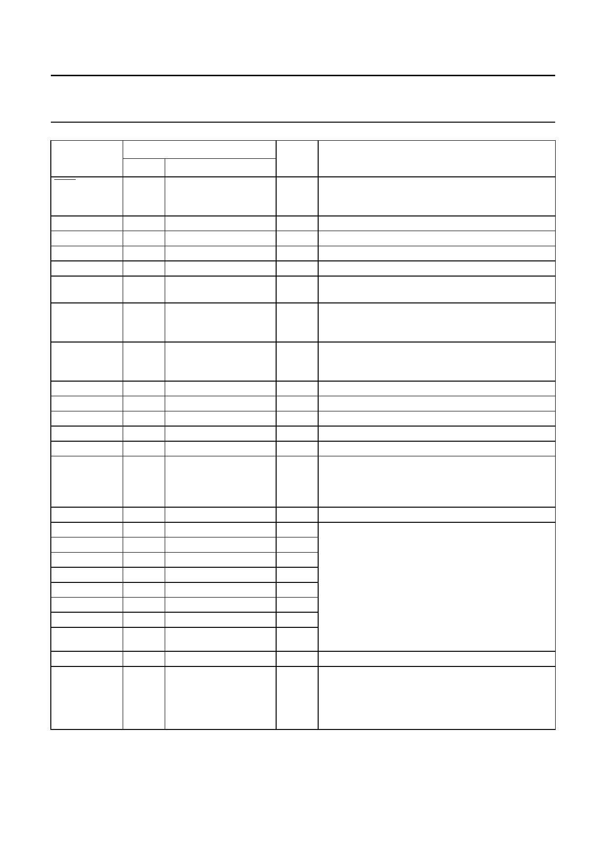
SYMBOL
COR
VDDA
B
G
R
VDS
HSYNC
VSYNC
VSSP
VDDC
OSCGND
XTALIN
XTALOUT
RESET
VDDP
P1.0/INT1
P1.1/T0
P1.2/INT0
P1.3/T1
P1.6/SCL0
P1.7/SDA0
P1.4/SCL1
P1.5/SDA1
VPE_2
n.c.
SDIP52
29
PIN
LQFP100
43
31
45
32
46
33
47
34
48
35
52
36
53
37
55
38
12, 60
39
63
40
69
41
70
42
71
43
73
44
75
45
76
46
78
47
79
48
80
49
81
50
82
51
83
52
84
−
62
−
3, 7 to 10, 14, 15,
19 to 21, 23, 26, 27, 33,
36 to 40, 49 to 51,
56 to 58, 61, 64 to 68,
72, 74, 77, 85 to 92, 99
TYPE
DESCRIPTION
O Open-drain, active LOW output which allows selective
contrast reduction of the TV picture to enhance a
mixed mode display.
− +3.3 V analog power supply
O Pixel rate output of the BLUE colour information.
O Pixel rate output of the GREEN colour information.
O Pixel rate output of the RED colour information.
O Video/data switch push-pull output for dot rate fast
blanking.
I Schmitt triggered input TTL version of the horizontal
sync pulse. The polarity of this pulse is programmable
by register bit TXT1.H POLARITY.
I Schmitt triggered input for a TTL version of the vertical
sync pulse. The polarity of this pulse is programmable
by register bit TXT1.V POLARITY.
− periphery ground
− +3.3 V core power supply
− crystal oscillator ground
I 12 MHz crystal oscillator input
O 12 MHz crystal oscillator output
I If the reset input is HIGH for at least 2 machine cycles
(24 oscillator periods) while the oscillator is running,
the device is reset. This pin should be connected to
VDDP via a capacitor.
− +3.3 V periphery power supply
I/O Port 1. 8-bit programmable bidirectional port with
I/O alternative functions.
I/O P1.0/INT1 is external interrupt 1 which can be
I/O triggered on the rising and falling edge of the pulse.
I/O
P1.1/T0 is the Counter/Timer 0. P1.2/INT0 is external
interrupt 0. P1.3/T1 is the Counter/Timer 1.
I/O P1.6/SCL0 is the serial clock input for the I2C-bus and
I/O P1.7/SDA0 is the serial data port for the I2C-bus.
I/O P1.4/SCL1 is the serial clock input for the I2C-bus and
P1.5/SDA1 is the serial data port for the I2C-bus.
I OTP programming voltage
− not connected
2000 Feb 23
9
Share Link: