AD9814 데이터 시트보기 (PDF) - Analog Devices
부품명
상세내역
제조사
AD9814 Datasheet PDF : 15 Pages
| |||
AD9814
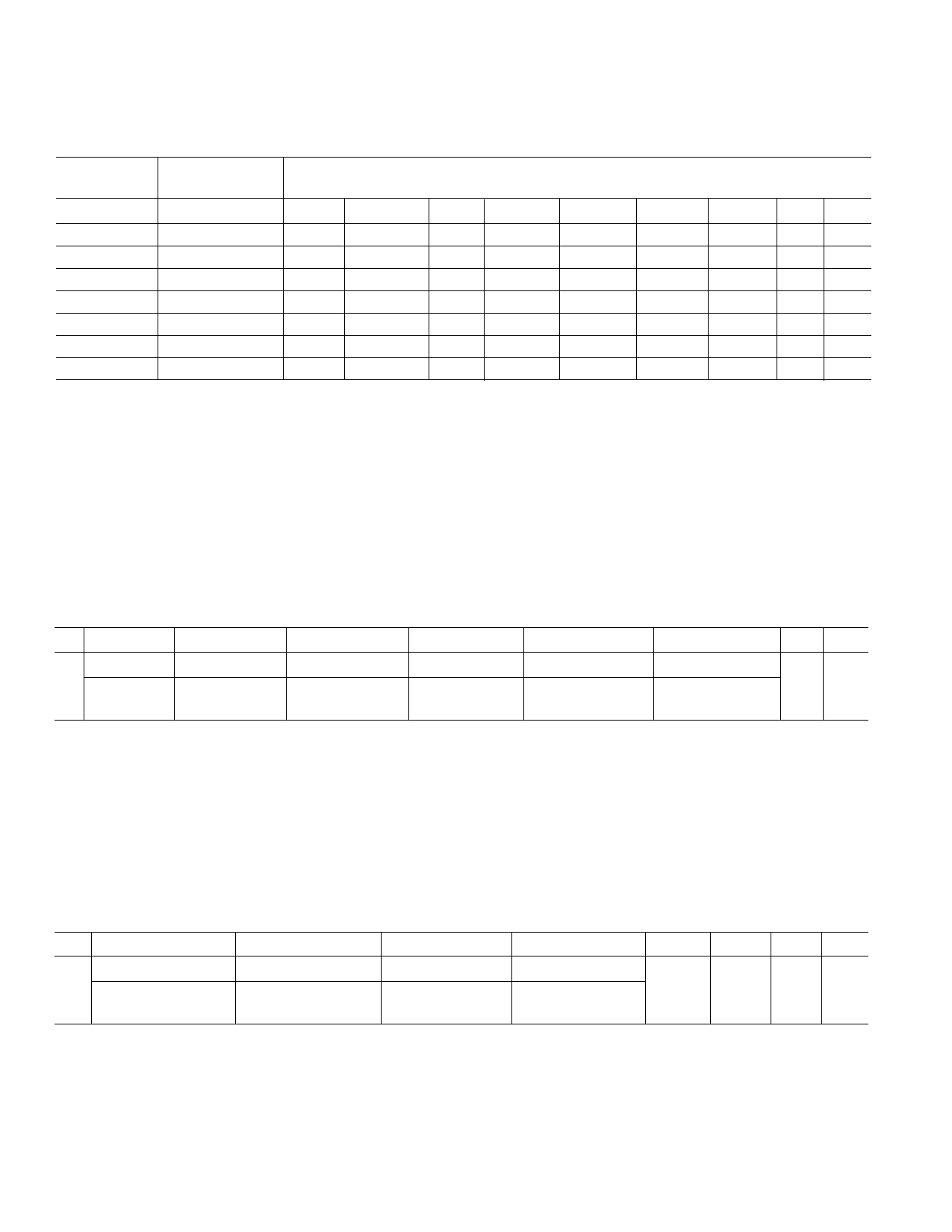
INTERNAL REGISTER DESCRIPTIONS
Register
Name
Configuration
MUX
Red PGA
Green PGA
Blue PGA
Red Offset
Green Offset
Blue Offset
Address
A2 A1 A0
00 0
00 1
01 0
01 1
10 0
10 1
11 0
11 1
D8
0
0
0
0
0
MSB
MSB
MSB
Table I. Internal Register Map
Data Bits
D7
D6 D5
D4
Input Rng
RGB/BGR
0
0
0
VREF
Red
0
0
0
3Ch/1Ch
Green
MSB
MSB
MSB
CDS On
Blue
D3
Clamp
0
D2
D1 D0
Pwr Dn 0 0
0
00
LSB
LSB
LSB
LSB
LSB
LSB
Configuration Register
The Configuration Register controls the AD9814’s operating mode and bias levels. Bits D8, D1 and D0 should always be set low. Bit
D7 sets the full-scale voltage range of the AD9814’s A/D converter to either 4 V (high) or 2 V (low). Bit D6 controls the internal
voltage reference. If the AD9814’s internal voltage reference is used, this bit is set high. Setting Bit D6 low will disable the internal
voltage reference, allowing an external voltage reference to be used. Bit D5 will configure the AD9814 for either the 3-Channel (high)
or 1-Channel (low) mode of operation. Setting Bit D4 high will enable the CDS mode of operation, and setting this bit low will en-
able the SHA mode of operation. Bit D3 sets the dc bias level of the AD9814’s input clamp. This bit should always be set high for
the 4 V clamp bias, unless a CCD with a reset feedthrough transient exceeding 2 V is used. If the 3 V clamp bias level is used, the
peak-to-peak input signal range to the AD9814 is reduced to 3 V maximum. Bit D2 controls the power-down mode. Setting Bit D2
high will place the AD9814 into a very low power “sleep” mode. All register contents are retained while the AD9814 is in the pow-
ered-down state.
Table II. Configuration Register Settings
D8 D7
D6
D5
D4
D3
D2
D1 D0
Set Input Range Internal VREF # of Channels CDS Operation Input Clamp Bias Power-Down
Set Set
to 1 = 4 V*
0 0=2V
1 = Enabled*
0 = Disabled
1 = 3-Ch Mode* 1 = CDS Mode* 1 = 4 V*
0 = 1-Ch Mode 0 = SHA Mode 0 = 3 V
1 = On
to to
0 = Off (Normal)* 0
0
*Power-on default value.
MUX Register
The MUX Register controls the sampling channel order in the AD9814. Bits D8, D3, D2, D1, and D0 should always be set low. Bit
D7 is used when operating in 3-Channel Mode. Setting Bit D7 high will sequence the MUX to sample the red channel first, then the
green channel and then the blue channel. When in this mode, the CDSCLK2 pulse always resets the MUX to sample the red channel
first (see Timing Figure 1). When Bit D7 is set low, the channel order is reversed to blue first, green second and red third. The
CDSCLK2 pulse will always reset the MUX to sample the blue channel first. Bits D6, D5, and D4 are used when operating in
1-Channel Mode. Bit D6 is set high to sample the red channel. Bit D5 is set high to sample the green channel. Bit D4 is set high to
sample the blue channel. The MUX will remain stationary during 1-Channel Mode.
D8 D7
Set 3-Channel Select
to
1 = R-G-B*
0
0 = B-G-R
*Power-on default value.
Table III. MUX Register Settings
D6
1-Channel Select
1 = RED*
0 = Off
D5
D4
D3
1-Channel Select 1-Channel Select Set
1 = GREEN
1 = BLUE
to
0 = Off*
0 = Off*
0
D2 D1 D0
Set Set Set
to
to to
0
0
0
–10–
REV. 0
Share Link: 