VND5012AK-E 데이터 시트보기 (PDF) - STMicroelectronics
부품명
상세내역
제조사
VND5012AK-E
STMicroelectronics

VND5012AK-E Datasheet PDF : 13 Pages
| |||
VND5012AK-E
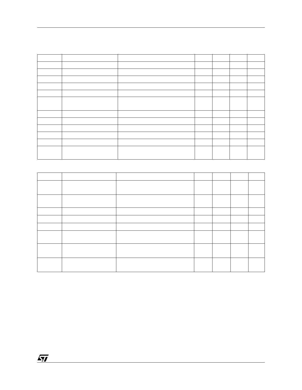
ELECTRICAL CHARACTERISTICS (continued)
Table 8. Logic Input
Symbol
Parameter
VIL
Input low level voltage
IIL
Low level input current
VIH
Input high level voltage
IIH
VI(hyst)
High level input current
Input hysteresis voltage
VICL
Input clamp voltage
VCSDL
ICSDL
VCSDH
ICSDH
VCSD(hyst)
CS_DIS low level voltage
Low level CS_DIS current
CS_DIS high level voltage
High level CS_DIS current
CS_DIS hysteresis voltage
VCSCL CS_DIS clamp voltage
Test Conditions
VIN=0.9 V
VIN= 2.1 V
IIN=1mA
IIN=-1mA
VCSD= 0.9V
VCSD= 2.1 V
ICSD=1mA
ICSD=-1mA
Min. Typ. Max. Unit
0.9
V
1
µA
2.1
V
10
µA
0.25
V
5.5
TBD
V
-0.7
V
0.9
V
1
µA
2.1
V
10
µA
0.25
V
5.5
TBD
V
-0.7
V
Table 9. Protections and Diagnostics (see note 2)
Symbol
Parameter
Test Conditions
Min. Typ. Max. Unit
IlimH
DC Short circuit current
VCC=13V
5V<VCC<36V
IlimL
Short circuit current
during thermal cycling
VCC=13V; TR<Tj<TTSD
40
60
80
A
80
A
24
A
TTSD
TR
TRS
THYST
VDEMAG
Shutdown temperature
Reset temperature
Thermal reset of STATUS
Thermal hysteresis
(TTSD-TR)
Turn-off output voltage
clamp
IOUT=2A; VIN=0; L=6mH
150
175
200
°C
TRS + 1 TRS + 5
°C
135
°C
7
°C
VCC-41 VCC-46 VCC-52 V
Output voltage drop
VON
limitation
IOUT=0.4A
Tj= -40°C...+150°C (see fig. 9)
25
mV
Note: 2. To ensure long term reliability under heavy overload or short circuit conditions, protection and related diagnostic signals must be
used together with a proper software strategy. If the device operates under abnormal conditions this software must limit the duration
and number of activation cycles.
5/13
Share Link: