VND5012AK-E 데이터 시트보기 (PDF) - STMicroelectronics
부품명
상세내역
제조사
VND5012AK-E
STMicroelectronics

VND5012AK-E Datasheet PDF : 13 Pages
| |||
VND5012AK-E
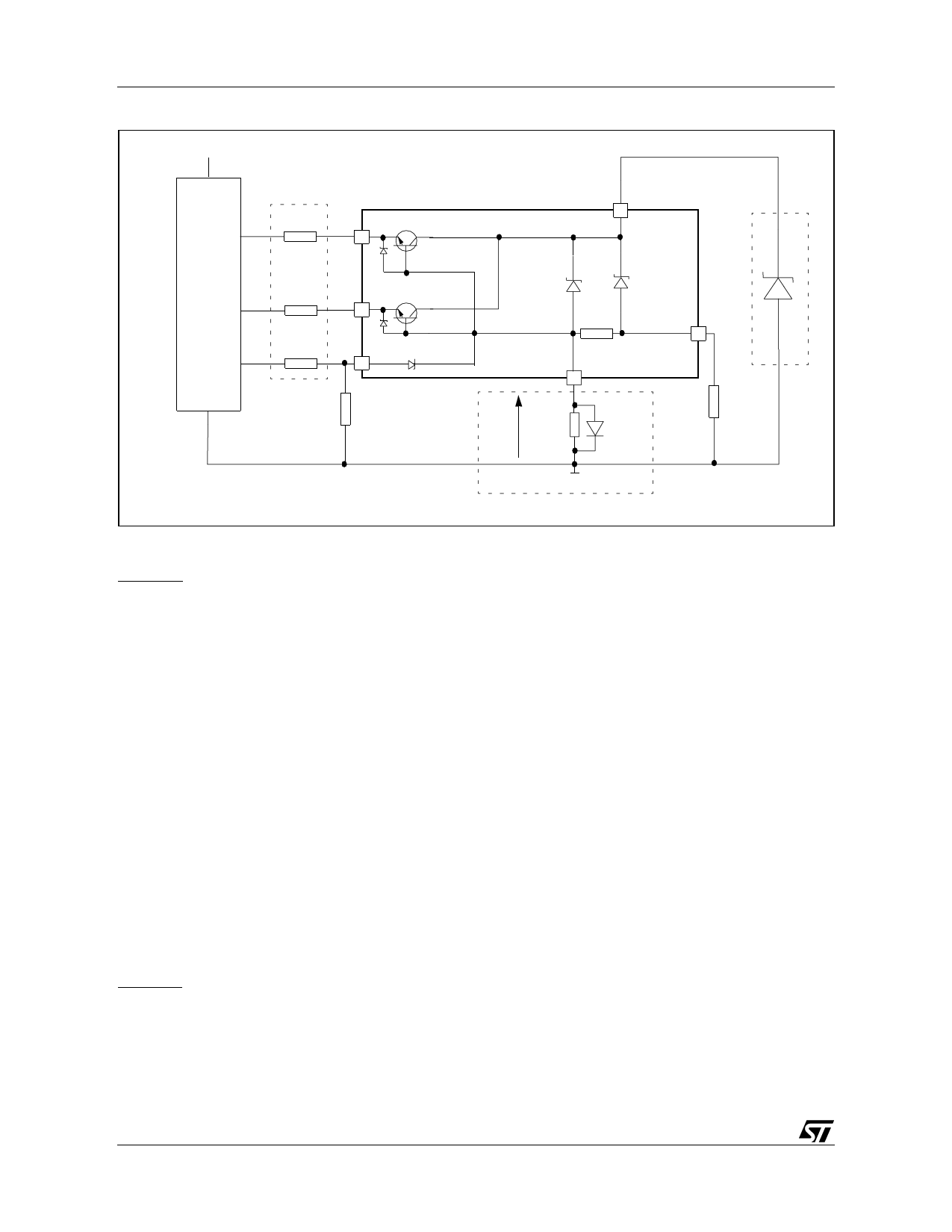
Figure 7. Application Schematic
+5V
Rprot
CS_DIS
VCC
Dld
µC
Rprot
Rprot
INPUT
CURRENT SENSE
GND
OUTPUT
RSENSE
VGND
RGND
DGND
Note: Channel 2 has the same internal circuit as channel 1.
GND PROTECTION NETWORK AGAINST
REVERSE BATTERY
Solution 1: Resistor in the ground line (RGND only). This
can be used with any type of load.
The following is an indication on how to dimension the
RGND resistor.
1) RGND ≤ 600mV / (IS(on)max).
2) RGND ≥ (−VCC) / (-IGND)
where -IGND is the DC reverse ground pin current and can
be found in the absolute maximum rating section of the
device datasheet.
Power Dissipation in RGND (when VCC<0: during reverse
battery situations) is:
PD= (-VCC)2/RGND
This resistor can be shared amongst several different
HSDs. Please note that the value of this resistor should
be calculated with formula (1) where IS(on)max becomes
the sum of the maximum on-state currents of the different
devices.
Please note that if the microprocessor ground is not
shared by the device ground then the RGND will produce a
shift (IS(on)max * RGND) in the input thresholds and the
status output values. This shift will vary depending on
how many devices are ON in the case of several high side
drivers sharing the same RGND.
If the calculated power dissipation leads to a large
resistor or several devices have to share the same
resistor then ST suggests to utilize Solution 2 (see
below).
Solution 2: A diode (DGND) in the ground line.
A resistor (RGND=1kΩ) should be inserted in parallel to
DGND if the device drives an inductive load.
This small signal diode can be safely shared amongst
several different HSDs. Also in this case, the presence of
the ground network will produce a shift (j600mV) in the
input threshold and in the status output values if the
microprocessor ground is not common to the device
ground. This shift will not vary if more than one HSD
shares the same diode/resistor network.
LOAD DUMP PROTECTION
Dld is necessary (Voltage Transient Suppressor) if the
load dump peak voltage exceeds the VCC max DC rating.
The same applies if the device is subject to transients on
the VCC line that are greater than the ones shown in the
ISO T/R 7637/1 table.
µC I/Os PROTECTION:
If a ground protection network is used and negative
transient are present on the VCC line, the control pins will
be pulled negative. ST suggests to insert a resistor (Rprot)
in line to prevent the µC I/Os pins to latch-up.
The value of these resistors is a compromise between the
leakage current of µC and the current required by the
HSD I/Os (Input levels compatibility) with the latch-up
limit of µC I/Os.
-VCCpeak/Ilatchup ≤ Rprot ≤ (VOHµC-VIH-VGND) / IIHmax
Calculation example:
For VCCpeak= - 100V and Ilatchup ≥ 20mA; VOHµC ≥ 4.5V
5kΩ ≤ Rprot ≤ 65kΩ.
Recommended Rprot value is 10kΩ.
8/13
Share Link: