MPSA55RLRA 데이터 시트보기 (PDF) - ON Semiconductor
부품명
상세내역
제조사
MPSA55RLRA Datasheet PDF : 8 Pages
| |||
MPSA05, MPSA06, MPSA55, MPSA56
ELECTRICAL CHARACTERISTICS (TA = 25°C unless otherwise noted)
Characteristic
Symbol
Min
OFF CHARACTERISTICS
Collector −Emitter Breakdown Voltage (Note 2.)
(IC = 1.0 mAdc, IB = 0)
V(BR)CEO
MPSA05, MPSA55
60
MPSA06, MPSA56
80
Emitter −Base Breakdown Voltage (IE = 100 µAdc, IC = 0)
Collector Cutoff Current (VCE = 60 Vdc, IB = 0)
Collector Cutoff Current
(VCB = 60 Vdc, IE = 0)
(VCB = 80 Vdc, IE = 0)
ON CHARACTERISTICS
V(BR)EBO
4.0
ICES
−
ICBO
MPSA05, MPSA55
−
MPSA06, MPSA56
−
DC Current Gain
(IC = 10 mAdc, VCE = 1.0 Vdc)
(IC = 100 mAdc, VCE = 1.0 Vdc)
Collector −Emitter Saturation Voltage
(IC = 100 mAdc, IB = 10 mAdc)
hFE
100
100
VCE(sat)
−
Base−Emitter On Voltage
(IC = 100 mAdc, VCE = 1.0 Vdc)
SMALL−SIGNAL CHARACTERISTICS
VBE(on)
−
Current −Gain − Bandwidth Product (Note 3.)
(IC = 10 mA, VCE = 2.0 V, f = 100 MHz)
(IC = 100 mAdc, VCE = 1.0 Vdc, f = 100 MHz)
fT
MPSA05
100
MPSA06
MPSA55
50
MPSA56
2. Pulse Test: Pulse Width v 300 ms, Duty Cycle v 2%.
3. fT is defined as the frequency at which |hfe| extrapolates to unity.
Max
Unit
Vdc
−
−
−
Vdc
0.1
µAdc
µAdc
0.1
0.1
−
−
−
0.25
Vdc
1.2
Vdc
MHz
−
−
5.0 ms
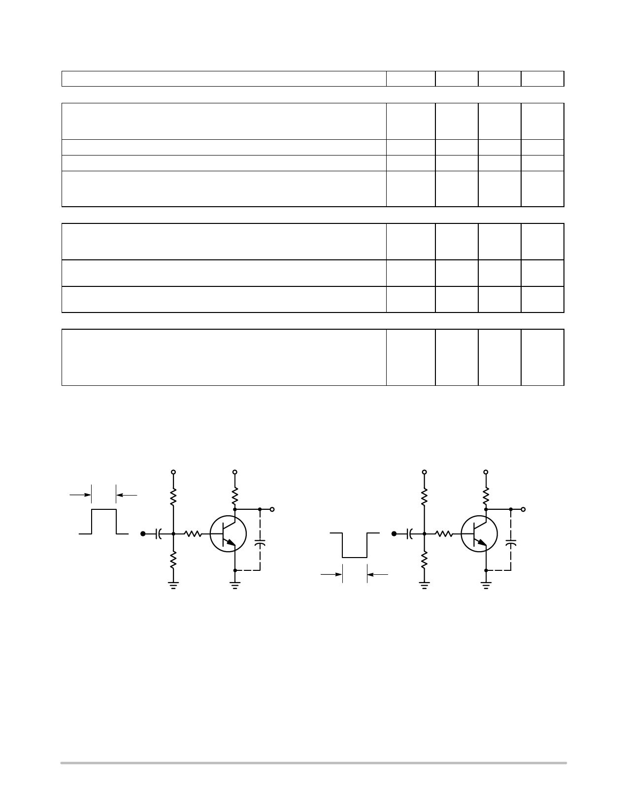
+10 V
0
tr = 3.0 ns
TURN−ON TIME
−1.0 V
VCC
+40 V
TURN−OFF TIME
+VBB
VCC
+40 V
100
Vin
RB
5.0 mF
100
RL
OUTPUT
* CS t 6.0 pF
5.0 ms
tr = 3.0 ns
100
Vin
RB
5.0 mF
100
RL
OUTPUT
* CS t 6.0 pF
*Total Shunt Capacitance of Test Jig and Connectors
For PNP Test Circuits, Reverse All Voltage Polarities
Figure 1. Switching Time Test Circuits
http://onsemi.com
2
Share Link: 