CDP6872E 데이터 시트보기 (PDF) - Intersil
부품명
상세내역
제조사
CDP6872E Datasheet PDF : 15 Pages
| |||
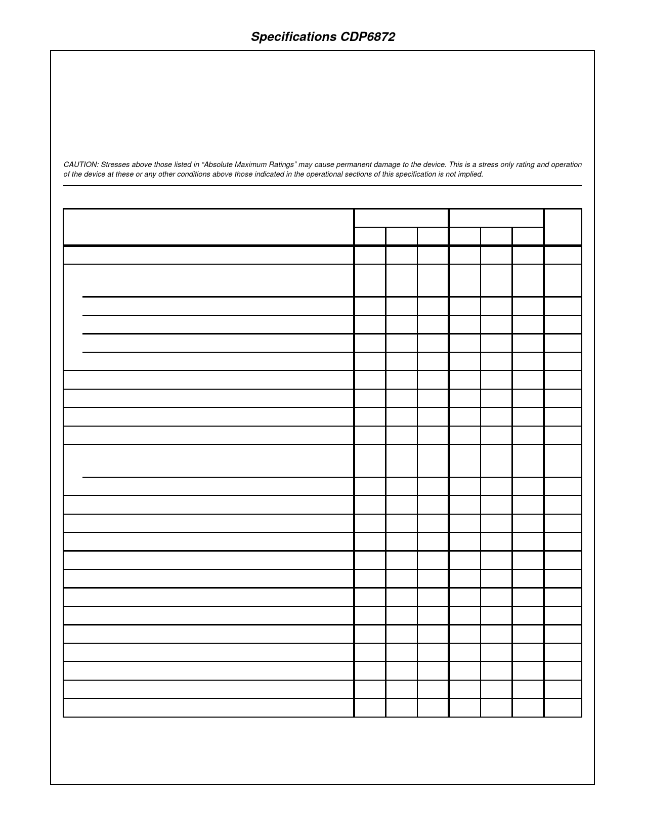
Specifications CDP6872
Absolute Maximum Ratings
Operating Conditions
Supply Voltage . . . . . . . . . . . . . . . . . . . . . . . . . . . . . . . . . . . . . 10.0V
Voltage (any pin). . . . . . . . . . . . . . . . . . . . . . .VSS-0.3V to VDD+0.3V
Junction Temperature (Plastic Package) . . . . . . . . . . . . . . . +150oC
ESD Rating (Note 2). . . . . . . . . . . . . . . . . . . . . . . . . . . . . . . >4000V
Lead Temperature (Soldering 10s) . . . . . . . . . . . . . . . . . . . . +300oC
(SOIC - Lead Tip Only)
Operating Temperature (Note 3) . . . . . . . . . . . . . . . . -40oC to +85oC
Storage Temperature Range. . . . . . . . . . . . . . . . . . -65oC to +150oC
Thermal Information (Typical)
Thermal Resistance (oC/W)
θJA
8 Lead Plastic DIP . . . . . . . . . . . . . . . . . . . . . . . . . . . . 125
8 Lead Plastic SOIC . . . . . . . . . . . . . . . . . . . . . . . . . . 170
CAUTION: Stresses above those listed in “Absolute Maximum Ratings” may cause permanent damage to the device. This is a stress only rating and operation
of the device at these or any other conditions above those indicated in the operational sections of this specification is not implied.
Electrical Specifications VSS = GND, TA = +25oC, Unless Otherwise Specified
PARAMETER
VDD = 5V
MIN TYP MAX
VDD = 3V
MIN TYP MAX
UNITS
VDD Supply Range (fOSC = 32kHz)
2
5
7
-
-
IDD Supply Current
fOSC = 32kHz, EN = 0 Standby
-
5.0 9.0
-
-
fOSC = 32kHz, CL = 10pF (Note 1), EN = 1, Freq1 = 1, Freq2 = 1
-
5.2 10.2
-
3.6
fOSC = 32kHz, CL = 40pF, EN = 1, Freq1 = 1, Freq2 = 1
-
10
15
-
6.5
fOSC = 1MHz, CL = 10pF (Note 1), EN = 1, Freq1 = 0, Freq2 = 1
-
130 200
-
90
fOSC = 1MHz, CL = 40pF, EN = 1, Freq1 = 0, Freq2 = 1
-
270 350
-
180
VOH Output High Voltage (IOUT = -1mA)
4.0 4.9
-
-
2.8
VOL Output Low Voltage (IOUT = 1mA)
-
0.07 0.4
-
0.1
IOH Output High Current (VOUT ≥ 4V)
-
-10
-5
-
-
IOL Output Low Current (VOUT ≤ 0.4V)
5.0 10.0
-
-
-
Three-State Leakage Current
(VOUT = 0V, 5V, TA = 25oC, -40oC)
(VOUT = 0V, 5V, TA = 85oC)
-
0.1
-
-
-
-
10
-
-
-
IIN Enable, Freq1, Freq2 Input Current (VIN = VSS to VDD)
-
0.4 1.0
-
-
VIH Input High Voltage Enable, Freq1, Freq2
2.0
-
-
-
-
VIL Input Low Voltage Enable, Freq1, Freq2
-
-
0.8
-
-
Enable Time (CL = 18pF, RL = 1kΩ)
-
800
-
-
-
Disable Time (CL = 18pF, RL = 1kΩ)
-
90
-
-
-
tR Output Rise Time (10% - 90%, fOSC = 32kHz, CL = 40pF)
-
12
25
-
12
tF Output Fall Time (10% - 90%, fOSC = 32kHz, CL = 40pF)
-
12
25
-
14
Duty Cycle (CL = 40pF) fOSC = 1MHz, Packaged Part Only (Note 4)
40
54
60
-
-
Duty Cycle (CL = 40pF) fOSC = 32kHz, (See Typical Curves)
-
41
-
-
44
Frequency Stability vs. Supply Voltage (fOSC = 32kHz, VDD = 5V, CL=10pF) -
1
-
-
-
Frequency Stability vs. Temperature (fOSC = 32kHz, VDD = 5V, CL=10pF)
-
0.1
-
-
-
Frequency Stability vs. Load (fOSC = 32kHz, VDD = 5V, CL=10pF)
-
0.01
-
-
-
NOTES:
1. Calculated using the equation IDD = IDD (No Load) + (VDD) (fOSC)(CL)
2. Human body model.
3. This product is production tested at +25oC only.
4. Duty cycle will vary with supply voltage, oscillation frequency, and parasitic capacitance on the crystal pins.
-
V
-
µA
6.1
µA
9
µA
180
µA
270
µA
-
V
-
V
-
mA
-
mA
-
nA
-
nA
-
µA
-
V
-
V
-
ns
-
ns
-
ns
-
ns
-
%
-
%
- ppm/V
- ppm/oC
- ppm/pF
3
Share Link: 