M63015FP 데이터 시트보기 (PDF) - MITSUBISHI ELECTRIC
부품명
상세내역
제조사
M63015FP Datasheet PDF : 15 Pages
| |||
MITSUBISHI SEMICONDUCTOR (LSI)
M63015FP
SPINDLE MOTOR AND 4CH ACTUATOR DRIVER
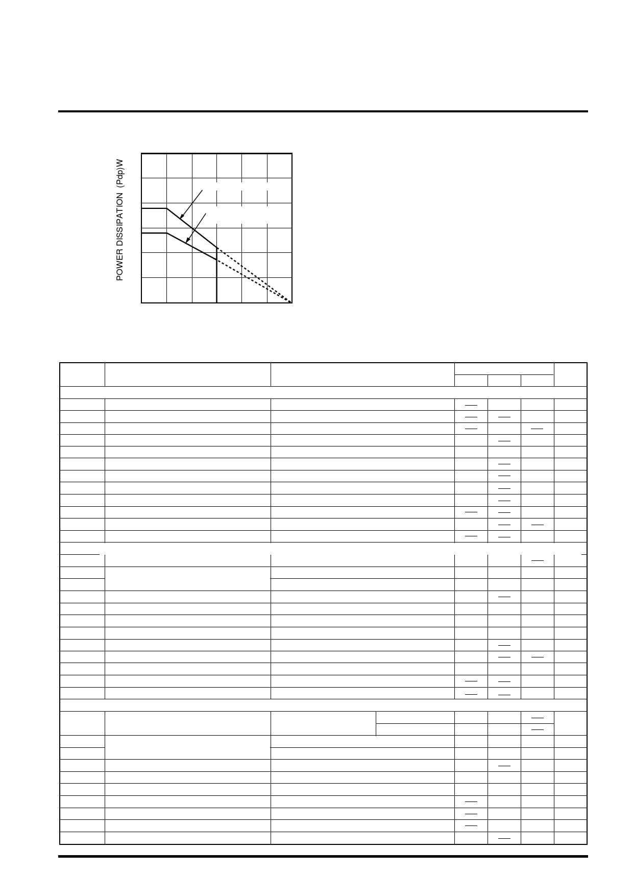
TYPICAL CHARACTERISTICS
6.0
5.0
Using N-type board:3.6W
4.0
Using P-type,O-type
board:2.6W
3.0
2.0
This IC's package is POWER-SSOP, so
improving the board on which the IC is
mounted enables a large power dissipation
without a heat sink.
For example, using an 1 layer glass epoxy
resin board, the IC's power dissipation is
2.6W at least. And it comes to 3.6W by
using an improved 2 layer board.
The information of the N, P, O type board is
shown in attached.
1.0
0
0 25 50 75 100 125 150
AMBIENT TEMPERATURE Ta (˚C)
ELECTRICAL CHARACTERISTICS (Ta=25˚C, 5VCC=VM4=5V,VM1=VM23=12V unless otherwise noted.)
Symbol
Parameter
Common
Icc1
Icc2
Fosc
VinOP
IinOP
VofOP
VoutOP
VinREF
IinREF
VMULO
VMUHI
IMU
Spindle
Vdyc1
Vdead1-
Vdead1+
Vin1
Gvo1
Vlim1F
Vlim1R
VHcom
VHmin
VHB
IHB
Supply current
Sleep current
PWM carrier frequency
OPamp input voltage range
OPamp input current
OPamp input offset voltage
OPamp output voltage range
REF input voltage range
REF input voltage range
MUTE terminal low voltage
MUTE terminal high voltage
Mute terminal input current
Dynamic range of output
Control voltage dead zone1
Control voltage input range 1
Control gain 1
Control limit 1F
Control limit 1R
Hall sensor amp.common mode input range
Hall sensor amp.input signal level
HB output voltage
HB terminal sink current
Test conditions
Limits
Min. Typ.
5VCC,VM1, VM23, VM4 current
5VCC,VM1, VM23, VM4 current under Sleep (MU1 = MU2 =0V).
OSC : with 180pF
OPIN-
OPIN-=1.65V
REF=1.65V(OPIN-=OPOUT ;buffer)
Io=-2.0~+2.0mA
VREF=1.65V
MU1,MU2
MU1,MU2
MU1,MU2 at 5V input voltage
60
110
-0
-1.0 -0.15
-10
0.5
1.0
-10
3.0
Io=0.5 [A]
SPIN<REF [REVERSE]
REF<SPIN [FORWARD]
SPIN
Gio1=Gvo1/ Rs [A/V]
Ilim1F=Vlim1F/ Rs [A] [FORWARD]
Ilim1R=Vlim1R/ Rs [A] [REVERSE]
Hu+,Hu-,Hv+,Hv-,Hw+ ,Hw-
Hu+,Hu-,Hv+,Hv-,Hw+ ,Hw-
at Load current (IHB)=10mA
MU1=MU2=0V or MU1=MU2=5V orMU1=5V/MU2=0V
10.3
-80
0
0
0.85
0.4
0.27
1.3
60
0.6
10.8
-40
+40
1.0
0.5
0.34
0.85
FGD
Slide
FG duty
Vdyc2 Dynamic range of output
Vdead2-
Vdead2+
Vin2
Gvo2
Vlim2
Tdon
Tdoff
Tdsw
Ileak
Control voltage dead zone 2
Control voltage input range 2
Control gain 2
Control limit 2
Output turn-on delay
Output turn-off delay
Output switching delay
Output leak current
at FG frequency=3kHz,hall input signal level 80mVp-p
Io=0.5 [A]
at VM23=5[V]
at VM23=12[V]
SLIN < REF
REF < SLIN
SLIN
Gio2=Gvo2/ Rs [A/V]
Ilim2=Vlim2/ Rs [A]
The time taken to turn on the output after the Rs voltage goes above the
command value.
The time taken to turn off the output after the Rs voltage goes down the
command value.
The time when all the output Tr.s are turned off during the switching of the
output Tr.
MU1=MU2=5v,MU1=MU2=0v
3.3
10.3
-80
0
0
0.85
0.43
-100
3.8
10.8
-40
+40
1.0
0.5
1.0
3.5
5.0
Max. Unit
78 mA
30 µA
KHz
5
V
0 µA
+10 mV
4.5
V
3.3
V
+10 µA
0.8
V
V
500 µA
V
0 mV
+80 mV
5
V
1.15 V/V
0.6
V
0.41
V
3.7
V
mVp-p
1.2
V
30 mV
30 mV
V
0 mV
+80 mV
5
V
1.15 V/V
0.58
V
2.0 µsec
7.0 µsec
10.0 µsec
100 µA
Share Link: 