PNX4901 데이터 시트보기 (PDF) - NXP Semiconductors.
부품명
상세내역
제조사
PNX4901 Datasheet PDF : 2 Pages
| |||
The result is a phone that offers highly desirable features at
a dramatically lower price point than previously achievable,
and expanding the reach of these technologies to millions
more consumers in emerging and developed markets.
The PNX4902 lets OEMs and ODMs differentiate themselves
and their products in a fiercely competitive market.
Industry-leading integration and performance
As part of the PNX490x family, NXP’s family of innovative
single-chip GSM/GPRS solutions, the PNX4902 continues
to provide industry-leading integration, best-in-class RF
performance and power consumption, and an R99-compliant
communications protocol stack that is field-tested on more
than 100 networks across all major geographic markets.
The very high level of integration dramatically reduces
the number of external components. The only external ICs
necessary are a power amplifier and memory. A complete
triband GSM/GPRS modem can be created with just 50
external components, including passives and other discretes.
A better end-user experience
Several features of NXP’s highly integrated core architecture
let the PNX4902 deliver a more enjoyable end-user experience.
The PNX490x series is the only set of single-chip solutions that
obtains such a high level of integration while maintaining best-
in-class RF performance. They deliver significant margin to key
GSM specs across commonly encountered stress conditions in
the field, including extreme temperature and battery voltage.
They maintain excellent call quality in congested, urban
environments as well as in remote areas with sparse network
coverage. Additional features, such as SAIC, boost network
capacity even further. Superior echo cancellation and excellent
noise suppression make every call clearer, even in public spaces
and other noisy environments.
Plus, industry-leading power consumption means the battery
lasts longer, so consumers can spend more time talking
between battery recharges. With a small, inexpensive 600-mAh
battery, five hours of talk time and over 420 hours of standby
time are possible.
For the fastest possible time-to-market, the PNX4902 hardware
reference design is accompanied by a flexible, pre-integrated, and
fully validated software solution that also reduces R&D expenses.
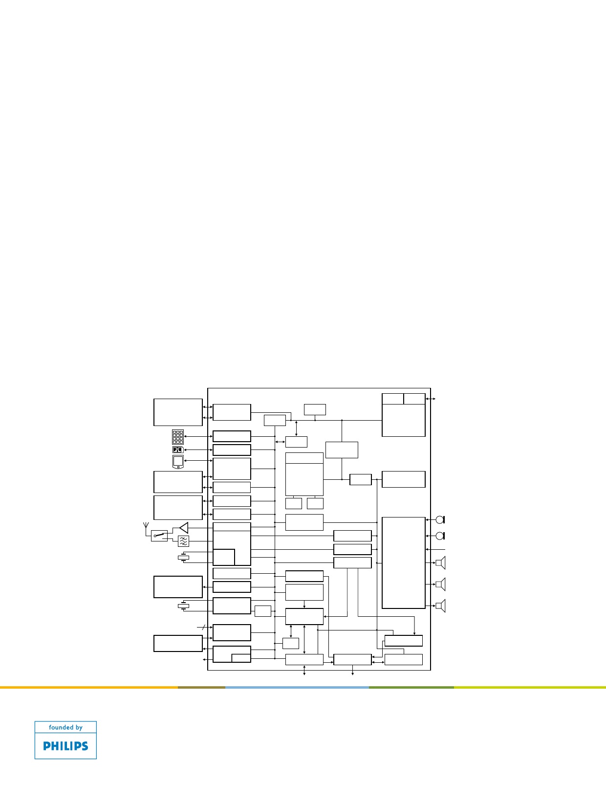
PNX4902 block diagram
FLASH
RAM
LCD
CO-PROCESSOR
123
456
789
* 0#
BLUETOOTH
SD/MMC
LCD
FM TUNER
VIBRATOR
BACKLIGHT
BUZZER
2
BATTERY
SUBSYSTEM
PNX4902
EBI
ROM
BRIDGE
AHB
KEYPAD
SIM I/F
UART(2)
PCM
SSI
I2C
PA ramp DAC
RF
SUBSYSTEM
DCXO
HW SECURITY
PWM(3)
RTC
SCC
AUX ADC's
PMU
PSEQ
DMA
D_JTAG
HOST
INTERFACE
Ceva-Teak
DSP
BRIDGE
ROM RAM
POWER
CONTROL
SYSCONFIG
TIMERS
(WD, GP)
INTERRUPT
CONTROLLER
RFTX
RFRX
RTEC
SMC
GPIO
DEBUG
ETM9 JTAG
ARM926EJ-S
MCU
DSP
ACCELERATORS
AUDIO
SUBSYSTEM
Int
Ext
AUX
Handset
Headset
Loadspeaker
HSL
DAI
brb158
www.nxp.com
© 2008 NXP B.V.
All rights reserved. Reproduction in whole or in part is prohibited without the prior written consent of the copyright owner.
The information presented in this document does not form part of any quotation or contract, is believed to be accurate and
reliable and may be changed without notice. No liability will be accepted by the publisher for any consequence of its use.
Publication thereof does not convey nor imply any license under patent- or other industrial or intellectual property rights.
Date of release: January 2008
Document order number: 9397 750 16248
Printed in the Netherlands
Share Link: 