SA534D 데이터 시트보기 (PDF) - Philips Electronics
부품명
상세내역
제조사
SA534D Datasheet PDF : 7 Pages
| |||
Philips Semiconductors
Low power quad op amps
Product specification
LM124/224/324/324A/
SA534/LM2902
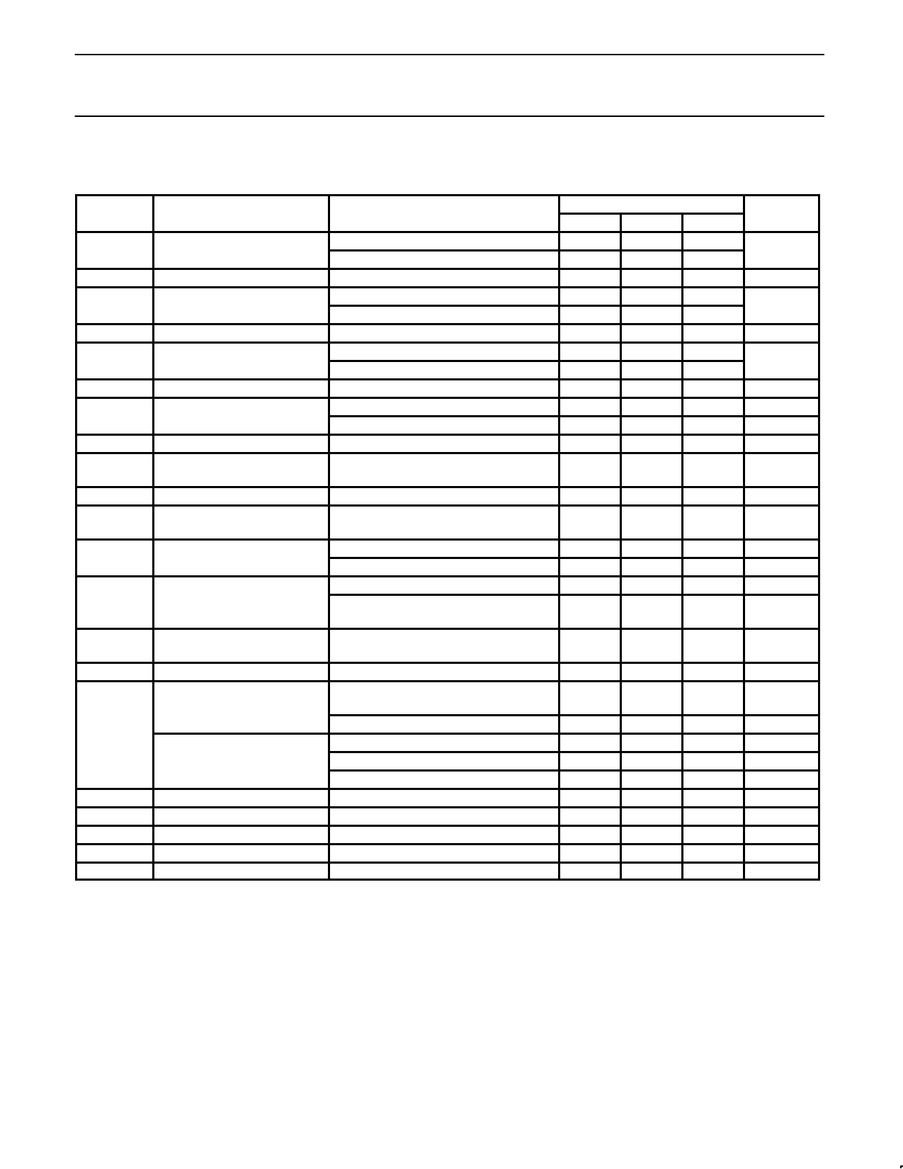
DC ELECTRICAL CHARACTERISTICS (Continued)
VCC=5V, TA=25°C unless otherwise specified.
SYMBOL
PARAMETER
TEST CONDITIONS
LM324A
Min
Typ
Max
UNIT
VOS
∆VOS/∆T
IBIAS
∆IBIAS/∆T
IOS
∆IOS/∆T
VCM
Offset voltage1
Temperature drift
Input current2
Temperature drift
Offset current
Temperature drift
Common-mode voltage range3
CMRR
VOUT
Common-mode rejection ratio
Output voltage swing
RS=0Ω
RS=0Ω, over temp.
RS=0Ω, over temp.
IIN(+) or IIN(-)
IIN(+) or IIN(-), over temp.
Over temp.
IIN(+)-IIN(-)
IIN(+)-IIN(-), over temp.
Over temp.
VCC≤30V
VCC≤30V, over temp.
VCC=30V
RL=2kΩ, VCC=30V,
over temp.
±2
±3
mV
±5
7
30
µV/°C
45
100
nA
40
200
50
pA/°C
±5
±30
±75
nA
10
300
pA/°C
0
VCC-1.5
V
0
VCC-2
V
65
85
dB
26
V
VOH
Output voltage high
VOL
Output voltage low
RL≤10kΩ, VCC=30V, over temp.
RL≤10kΩ,
over temp.
27
28
V
5
20
mV
ICC
AVOL
Supply current
Large-signal voltage gain
RL=∞, VCC=30V, over temp.
RL=∞, over temp.
VCC=15V (for large VO swing), RL≥2kΩ
25
VCC=15V (for large VO swing), RL≥2kΩ,
over temp.
15
1.5
3
0.7
1.2
100
mA
mA
V/mV
V/mV
Amplifier-to-amplifier coupling5
f=1kHz to 20kHz,
input referred
-120
dB
PSRR
Power supply rejection ratio
RS≤0Ω
65
100
dB
Output current
source
VIN+=+1V, VIN-=0V, VCC=15V
20
40
mA
IOUT
ISC
VDIFF
GBW
Output current
sink
Short-circuit current4
Differential input voltage3
Unity gain bandwidth
VIN+=+1V, VIN-=0V, VCC=15V, over temp.
10
VIN-=+1V, VIN+=0V, VCC=15V
10
VIN-=+1V, VIN+=0V, VCC=15V, over temp.
5
VIN-=+1V, VIN+=0V, VO=200mV
12
10
20
mA
20
mA
8
mA
50
µA
40
60
mA
VCC
V
1
MHz
SR
Slew rate
0.3
V/µs
VNOISE
Input noise voltage
f=1kHz
40
nV/√Hz
NOTES:
1. VO ≈ 1.4VDC, RS=0Ω with VCC from 5V to 30V and over full input common-mode range (0VDC+ to VCC -1.5V).
2. The direction of the input current is out of the IC due to the PNP input stage. This current is essentially constant, independent of the state of
the output so no loading change exists on the input lines.
3. The input common-mode voltage or either input signal voltage should not be allowed to go negative by more than 0.3V. The upper end of the
common-mode voltage range is VCC -1.5, but either or both inputs can go to +32V without damage.
4. Short-circuits from the output to VCC can cause excessive heating and eventual destruction. The maximum output current is approximately
40mA independent of the magnitude of VCC. At values of supply voltage in excess of +15VDC, continuous short-circuits can exceed the
power dissipation ratings and cause eventual destruction. Destructive dissipation can result from simultaneous shorts on all amplifiers.
5. Due to proximity of external components, insure that coupling is not originating via stray capacitance between these external parts. This
typically can be detected as this type of coupling increases at higher frequencies.
1995 Nov 27
4
Share Link: 