SSM2275 데이터 시트보기 (PDF) - Analog Devices
부품명
상세내역
제조사
SSM2275 Datasheet PDF : 16 Pages
| |||
SSM2275/SSM2475
This phase reversal can be prevented by limiting the input cur-
rent to +1 mA. This can be done by placing a resistor in series
with the input terminal that is expected to be overdriven. The
series resistance should be at least:
RIN
= VIN , MAX − 0.6
1 mA
(3)
An equivalent resistor should be placed in series with both in-
puts to prevent offset voltages due to input bias currents, as
shown in Figure 28.
Output Short Circuit Protection
To achieve high quality rail-to-rail performance, the output of
the SSM2275/SSM2475 is not short-circuit protected. Shorting
the output may damage or destroy the device when excessive
voltages or currents are applied. To protect the output stage, the
maximum output current should be limited to ± 40 mA. Placing
a resistor in series with the output of the amplifier as shown in
Figure 29, the output current can be limited. The minimum
value for RX can be found from Equation 4.
RX
=
VSY
40 mA
(4)
For a +5 V single supply application, RX should be at least
125 Ω. Because RX is inside the feedback loop, VOUT is not
affected. The trade off in using RX is a slight reduction in output
voltage swing under heavy output current loads. RX will also
increase the effective output impedance of the amplifier to
RO + RX, where RO is the output impedance of the device.
RFB
RX
FEEDBACK
125⍀
A1
VOUT
A1 = 1/2 SSM2275
Figure 29. Output Short Circuit Protection Configuration
Power Dissipation Considerations
While many designers are constrained to use very small and low
profile packages, reliable operation demands that the maximum
junction temperatures not be exceeded. A simple calculation
will ensure that your equipment will enjoy reliable operation
over a long lifetime. Modern IC design allows dual and quad
amplifiers to be packaged in SOIC and microSOIC packages,
but it is the responsibility of the designer to determine what the
actual junction temperature will be, and prevent it from exceed-
ing the 150°C. Note that while the θJC is similar between pack-
age options, the θJA for the SOIC and TSSOP are nearly double
the PDIP. The calculation of maximum ambient temperature is
relatively simple to make.
PMAX
= TI , MAX − TA
θ JA
(5)
For example, with the 8-lead SOIC, the calculation gives a
maximum internal power dissipation (for all amplifiers, worst
case) of PMAX = (150°C – 85°C)/158°C/W = 0.41 W. For the
DIP package, a similar calculation indicates that 0.63 W (ap-
proximately 50% more) can be safely dissipated. Note that am-
bient temperature is defined as the temperature of the PC board
to which the device is connected (in the absence of radiated or
convected heat loss). It is good practice to place higher power
devices away from the more sensitive circuits. When in doubt,
measure the temperature in the vicinity of the SSM2275 with a
thermocouple thermometer.
Maximizing Low Distortion Performance
Because the SSM2275/SSM2475 is a very low distortion amplifier,
careful attention should be given to the use of the device to prevent
inadvertently introducing distortion. Source impedances seen by
both inputs should be made equal, as shown in Figure 28, with
RB = R1ʈRF for minimum distortion. This eliminates any offset
voltages due to varying bias currents. Proper power supply
decoupling reduces distortion due to power supply variations.
Because the open loop gain of the amplifier is directly dependent
on the load resistance, loads of less than 10 kΩ will increase the
distortion of the amplifier. This is a trait of any rail-to-rail op
amp. Increasing load capacitance will also increase distortion.
It is recommended that any unused amplifiers be configured as a
unity gain follower with the noninverting input tied to ground.
This minimizes the power dissipation and any potential crosstalk
from the unused amplifier.
As with many FET-type amplifiers, the PMOS devices in the
input stage exhibit a gate-to-source capacitance that varies with
the common mode voltage. In an inverting configuration, the in-
verting input is held at a virtual ground and the common-mode
voltage does not vary. This eliminates distortion due to input
capacitance modulation. In noninverting applications, the gate-
to-source voltage is not constant, and the resulting capacitance
modulation can cause a slight increase in distortion.
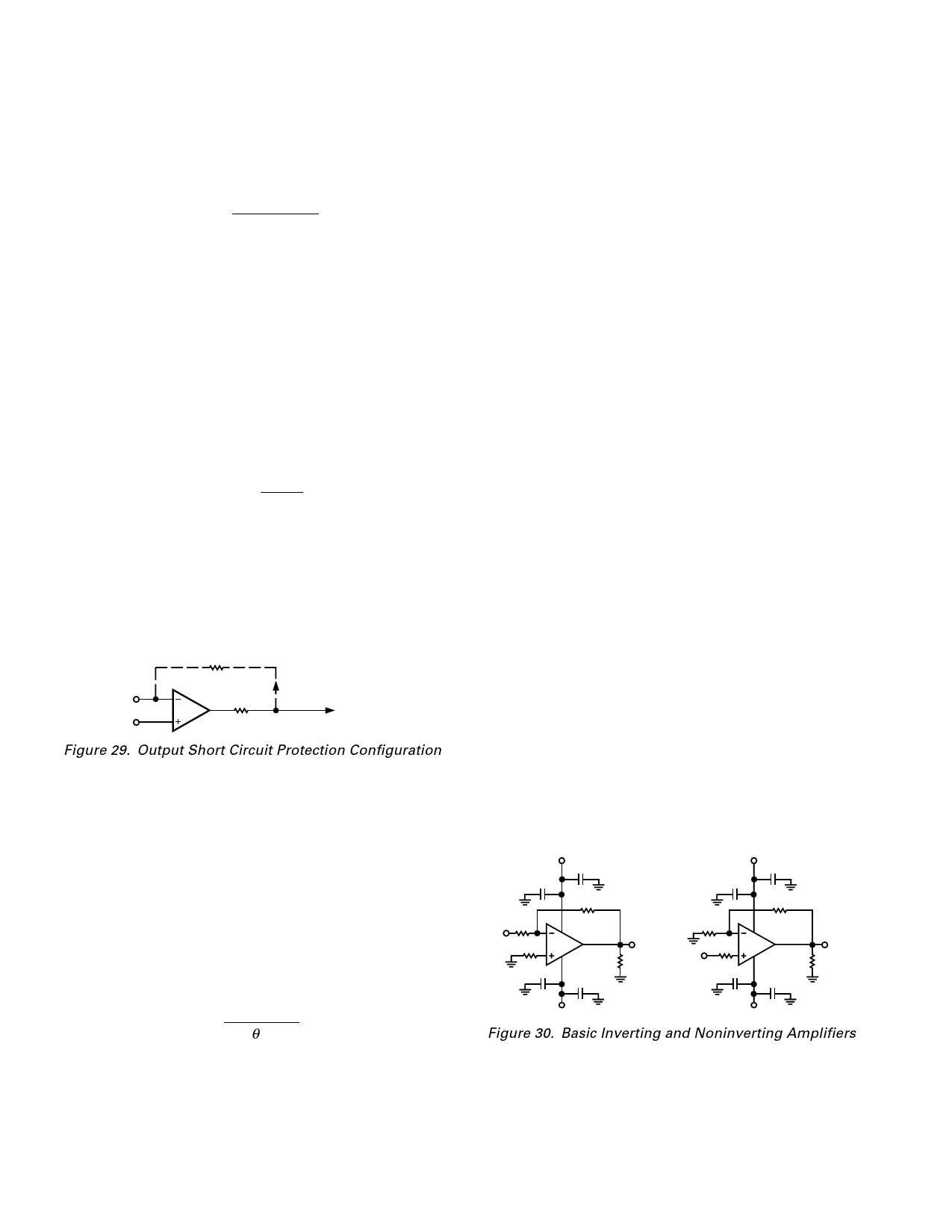
Figure 30 shows a unity gain inverter and a unity gain follower
configuration. Figure 31 shows an FFT of the outputs of these
amplifiers with a 1 kHz sine wave. Notice how the largest har-
monic amplitude (2nd harmonic) is –120 dB below the funda-
mental (0.0001%) in the inverting configuration.
V+
10F
0.1F
RFB
R1
VIN
RB
SSM2275
VOUT
RL
0.1F
10F
V+
10F
0.1F
RFB
R1
SSM2275
RB
VIN
0.1F
10F
VOUT
RL
V–
V–
Figure 30. Basic Inverting and Noninverting Amplifiers
–10–
REV. A
Share Link: 