SSM2275 데이터 시트보기 (PDF) - Analog Devices
부품명
상세내역
제조사
SSM2275 Datasheet PDF : 16 Pages
| |||
SSM2275/SSM2475
ABSOLUTE MAXIMUM RATINGS1
Supply Voltage (VS) . . . . . . . . . . . . . . . . . . . . . . . . . . . . ± 18 V
Input Voltage (VIN) . . . . . . . . . . . . . . . . . . . . . . . . . . . . ± 15 V
Differential Input Voltage2 . . . . . . . . . . . . . . . . . . . . . . . ± 15 V
Storage Temperature Range . . . . . . . . . . . . Ϫ65°C to ϩ150°C
Operating Temperature Range . . . . . . . . . . . Ϫ40°C to ϩ85°C
Junction Temperature Range . . . . . . . . . . . . Ϫ65°C to ϩ150°C
Lead Temperature Range (Soldering, 60 sec) . . . . . . . ϩ300°C
ESD Susceptibility . . . . . . . . . . . . . . . . . . . . . . . . . . . . 2,000 V
NOTES
1Stresses above those listed under Absolute Maximum Ratings may cause perma -
nent damage to the device. This is a stress rating only; the functional operation of
the device at these or any other conditions above those indicated in the operational
sections of this specification is not implied. Exposure to absolute maximum rating
conditions for extended periods may affect device reliability.
2For supplies less than ± 15 V, the input voltage and differential input voltage
must be less than ±15 V.
Package Type
8-Lead Plastic DIP
8-Lead SOIC
8-Lead microSOIC
14-Lead SOIC
14-Lead TSSOP
JA*
JC
Units
103
43
°C/W
158
43
°C/W
206
43
°C/W
120
36
°C/W
180
35
°C/W
*θJA is specified for the worst case conditions, i.e., for device in socket for DIP
packages and soldered onto a circuit board for surface mount packages.
Model
SSM2275P
SSM2275S
SSM2275RM
SSM2475S
SSM2475RU
Temperature
Range
–40°C to +85°C
–40°C to +85°C
–40°C to +85°C
–40°C to +85°C
–40°C to +85°C
ORDERING GUIDE
Package
Description
8-Lead PDIP
8-Lead SOIC
8-Lead microSOIC
14-Lead SOIC
14-Lead TSSOP
Package
Options
N-8
SO-8
RM-8
R-14
RU-14
CAUTION
ESD (electrostatic discharge) sensitive device. Electrostatic charges as high as 4000 V readily
accumulate on the human body and test equipment and can discharge without detection.
Although the SSM2275/SSM2475 features proprietary ESD protection circuitry, permanent
damage may occur on devices subjected to high energy electrostatic discharges. Therefore, proper
ESD precautions are recommended to avoid performance degradation or loss of functionality.
WARNING!
ESD SENSITIVE DEVICE
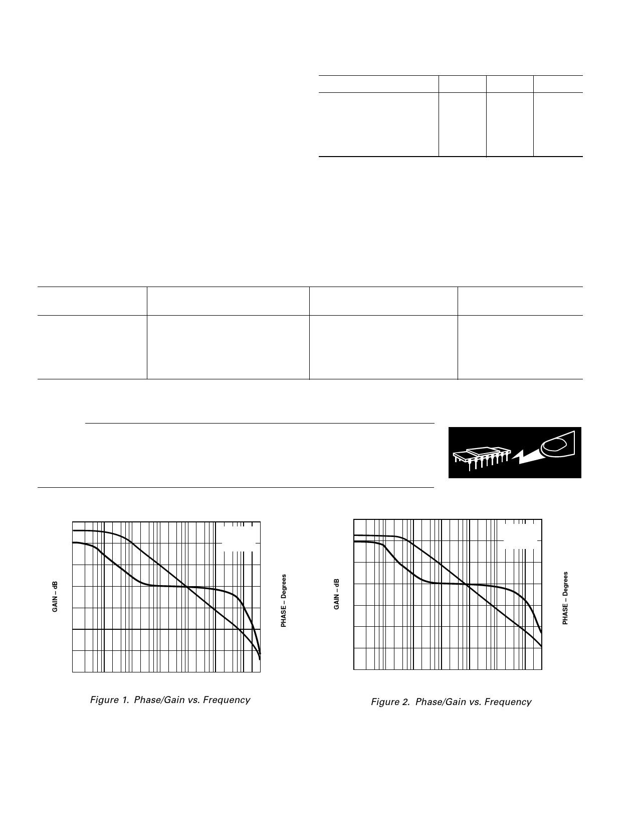
100
225
VS = ؎2.5V
RL = 2k⍀
80
CL = 10pF 180
60
135
40
90
20
45
0
0
–20
–45
–40
10
–90
100
1k
10k 100k
1M
10M 40M
FREQUENCY – Hz
Figure 1. Phase/Gain vs. Frequency
100
225
VS = ؎2.5V
80
RL = 600⍀
CL = 10pF
180
60
135
40
90
20
45
0
0
–20
–45
–40
10
–90
100
1k
10k
100k
1M
10M 40M
FREQUENCY – Hz
Figure 2. Phase/Gain vs. Frequency
–4–
REV. A
Share Link: 