EL2002ACN 데이터 시트보기 (PDF) - Elantec -> Intersil
부품명
상세내역
제조사
EL2002ACN Datasheet PDF : 12 Pages
| |||
EL2002C
Low Power 180 MHz Buffer Amplifier
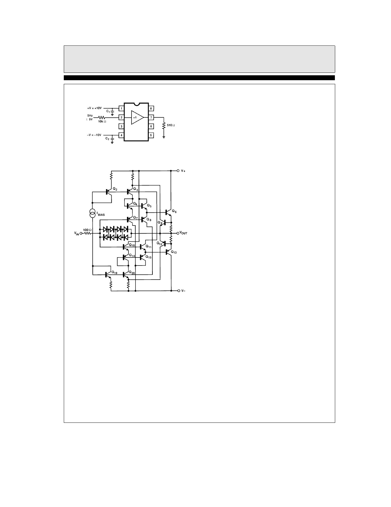
Burn-In Circuit
Power Supplies
The EL2002 may be operated with single or split
supplies with total voltage difference between
10V (g5V) and 36V (g18V) It is not necessary
to use equal split value supplies For example
b5V and a12V would be excellent for signals
from b2V to a9V
Simplified Schematic
Bypass capacitors from each supply pin to
2002 – 10
ground are highly recommended to reduce supply
ringing and the interference it can cause At a
minimum 1 mF tantalum capacitor with short
leads should be used for both supplies
2002 – 11
Application Information
The EL2002 is a monolithic buffer amplifier built
on Elantec’s proprietary Complementary Bipolar
process that produces NPN and PNP transistors
with essentially identical DC and AC character-
istics The EL2002 takes full advantage of the
complementary process with a unique circuit
topology
Elantec has applied for two patents based on the
EL2002’s topology The patents relate to the base
drive and feedback mechanism in the buffer This
feedback makes 2000 V ms slew rates with 100X
loads possible with very low supply current
Input Characteristics
The input to the EL2002 looks like a resistance in
parallel with about 3 5 pF in addition to a DC
bias current The DC bias current is due to the
miss-match in beta and collector current between
the NPN and PNP transistors connected to the
input pin The bias current can be either positive
or negative The change in input current with in-
put voltage (RIN) is affected by the output load
beta and the internal boost RIN can actually ap-
pear negative over portions of the input range
typical input current curves are shown in the
characteristic curves Internal clamp diodes from
the input to the output are provided These di-
odes protect the transistor base emitter junctions
and limit the boost current during slew to avoid
saturation of internal transistors The diodes be-
gin conduction at about g2 5V input to output
differential When that happens the input resist-
ance drops dramatically The diodes are rated at
50 mA When conducting they have a series re-
sistance of about 20X There is also 100X in series
with the input that limits input current Above
g7 5V differential input to output additional se-
ries resistance should be added
Source Impedance
The EL2002 has good input to output isolation
When the buffer is not used in a feedback loop
capacitive and resisitive sources up to 1 MHz
present no oscillation problems Care must be
used in board layout to minimize output to input
coupling CAUTION When using high source
impedances (RS l 100 kX) significant gain er-
rors can be observed due to output offset load
resistor and the action of the boost circuit See
typical performance curves
7
Share Link: 