LT1168IN8(RevA) 데이터 시트보기 (PDF) - Linear Technology
부품명
상세내역
제조사
LT1168IN8
(Rev.:RevA)
(Rev.:RevA)
Linear Technology

LT1168IN8 Datasheet PDF : 20 Pages
| |||
LT1168
ABSOLUTE AXI U RATI GS
(Note 1)
Supply Voltage ...................................................... ±20V
Differential Input Voltage (Within the
Supply Voltage) ..................................................... ±40V
Input Voltage (Equal to Supply Voltage) ................ ±20V
Input Current (Note 2) ....................................... ±20mA
Output Short-Circuit Duration (Note 3) ............ Indefinite
Operating Temperature Range (Note 4) .. – 40°C to 85°C
Specified Temperature Range
LT1168AC/LT1168C (Note 5) ............. – 40°C to 85°C
LT1168AI/LT1168I ............................. – 40°C to 85°C
Storage Temperature Range ................. – 65°C to 150°C
Lead Temperature (Soldering, 10 sec).................. 300°C
Order Options Tape and Reel: Add #TR
Lead Free: Add #PBF Lead Free Tape and Reel: Add #TRPBF
Lead Free Part Marking: http://www.linear.com/leadfree/
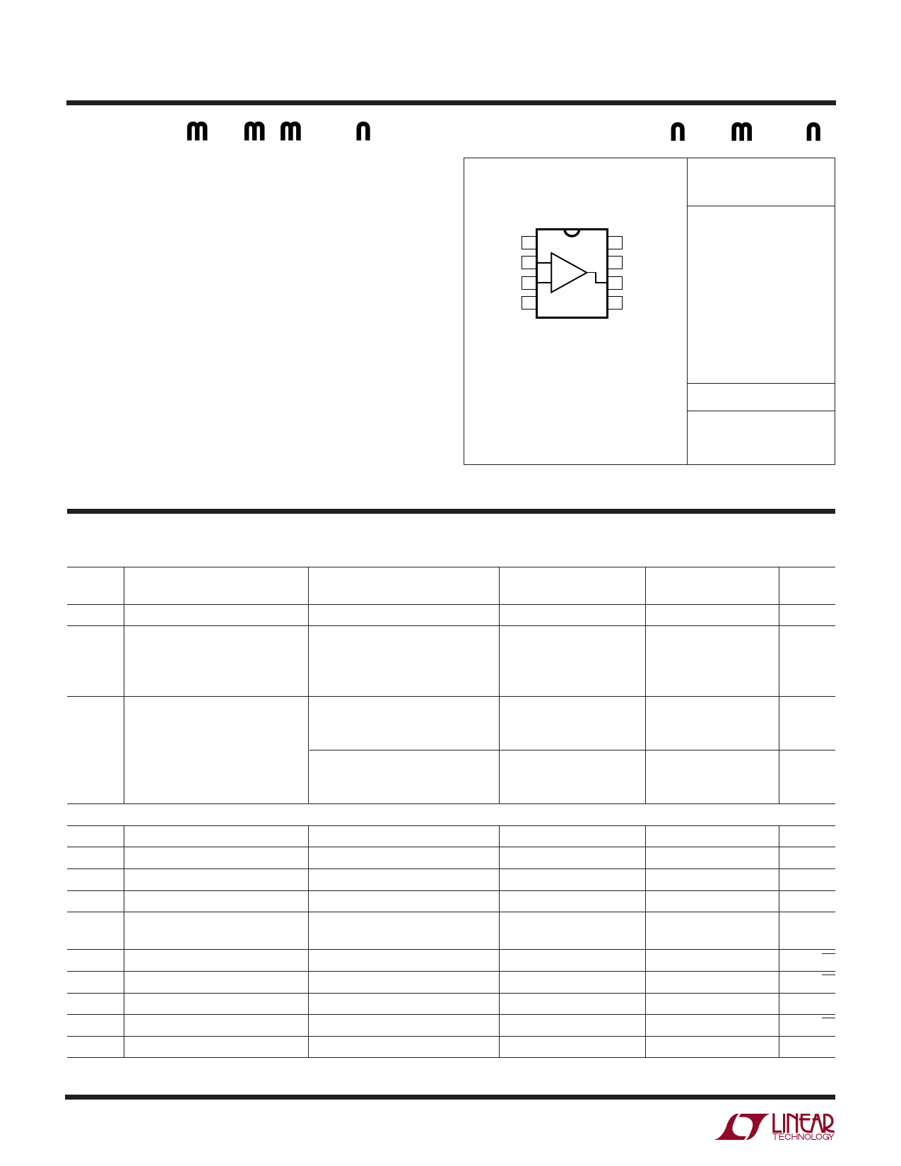
UW U
PACKAGE/ORDER I FOR ATIO
ORDER PART
NUMBER
TOP VIEW
RG 1
–IN 2 –
+IN 3 +
–VS 4
8 RG
7 +VS
6 OUTPUT
5 REF
N8 PACKAGE
8-LEAD PDIP
S8 PACKAGE
8-LEAD PLASTIC SO
TJMAX = 150°C, θJA = 150°C/ W (N8)
TJMAX = 150°C, θJA = 190°C/ W (S8)
LT1168ACN8
LT1168ACS8
LT1168AIN8
LT1168AIS8
LT1168CN8
LT1168CS8
LT1168IN8
LT1168IS8
S8 PART MARKING
1168A 1168
1168AI 1168I
Consult LTC Marketing for parts specified with wider operating temperature
ranges.
ELECTRICAL CHARACTERISTICS TA = 25°C. VS = ±15V, VCM = 0V, RL = 10k unless otherwise noted.
SYMBOL
G
VOST
VOSI
VOSO
IOS
IB
en
in
RIN
PARAMETER
CONDITIONS (Note 6)
Gain Range
Gain Error
G = 1 + (49.4k/RG)
G=1
G = 10 (Note 7)
G = 100 (Note 7)
G = 1000 (Note 7)
Gain Nonlinearity (Notes 7, 8)
VO = ±10V, G = 1
VO = ±10V,G = 10 and 100
VO = ±10V, G = 1000
VO = ±10V, G = 1, RL = 2k
VO = ±10V,G = 10 and 100, RL = 2k
VO = ±10V, G = 1000, RL = 2k
Total Input Referred Offset Voltage VOST = VOSI + VOSO/G
Input Offset Voltage
G = 1000, VS = ±5V to ±15V
Output Offset Voltage
G = 1, VS = ±5V to ±15V
Input Offset Current
Input Bias Current
Input Noise Voltage, RTI
0.1Hz to 10Hz, G = 1
0.1Hz to 10Hz, G = 1000
Input Noise Voltage Density, RTI
Output Noise Voltage Density, RTI
Input Noise Current
Input Noise Current Density
Input Resistance
fO = 1kHz
fO = 1kHz (Note 9)
fO = 0.1Hz to 10Hz
fO = 10Hz
VIN = ±10V
LT1168AC/LT1168AI
MIN TYP MAX
1
10k
0.008 0.02
0.04 0.4
0.04 0.5
0.08 0.5
2
6
10 20
20 40
4
15
20 40
40 75
15 40
40 200
50 300
40 250
2.00
0.28
10 15
165 220
5
74
300 1250
LT1168C/LT1168I
MIN TYP MAX
1
10k
0.015 0.03
0.05 0.5
0.05 0.6
0.08 0.6
3
10
15 25
25 60
5
20
30 60
50 90
20 60
50 300
60 450
80 500
2.00
0.28
10 15
165 220
5
74
200 1250
UNITS
%
%
%
%
ppm
ppm
ppm
ppm
ppm
ppm
µV
µV
pA
pA
µVP-P
µVP-P
nV/√Hz
nV/√Hz
pAP-P
fA/√Hz
GΩ
1168fa
2
Share Link: