FM24CL64B 데이터 시트보기 (PDF) - Cypress Semiconductor
부품명
상세내역
제조사
FM24CL64B Datasheet PDF : 18 Pages
| |||
FM24CL64B
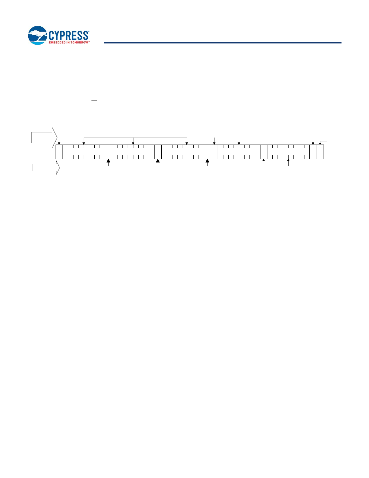
Selective (Random) Read
There is a simple technique that allows a user to select a random
address location as the starting point for a read operation. This
involves using the first three bytes of a write operation to set the
internal address followed by subsequent read operations.
To perform a selective read, the bus master sends out the slave
address with the LSB (R/W) set to 0. This specifies a write
operation. According to the write protocol, the bus master then
sends the address bytes that are loaded into the internal address
latch. After the FM24CL64B acknowledges the address, the bus
master issues a START condition. This simultaneously aborts
the write operation and allows the read command to be issued
with the slave address LSB set to a ‘1’. The operation is now a
current address read.
Start
By Master
Figure 12. Selective (Random) Read
Address
Start
Address
S
Slave Address 0 A
Address MSB
A
Address LSB
AS
Slave Address 1 A
No
Acknowledge
Stop
Data Byte
1P
By F-RAM
Acknowledge
Data
Endurance
The FM24C64B internally operates with a read and restore
mechanism. Therefore, endurance cycles are applied for each
read or write cycle. The memory architecture is based on an
array of rows and columns. Each read or write access causes an
endurance cycle for an entire row. In the FM24C64B, a row is 64
bits wide. Every 8-byte boundary marks the beginning of a new
row. Endurance can be optimized by ensuring frequently
accessed data is located in different rows. Regardless, FRAM
read and write endurance is effectively unlimited at the 1MHz I2C
speed. Even at 3000 accesses per second to the same segment,
10 years time will elapse before 1 trillion endurance cycles occur.
Document Number: 001-84458 Rev. *I
Page 8 of 18
Share Link: 