M29W320DB70N1E_03 데이터 시트보기 (PDF) - STMicroelectronics
부품명
상세내역
제조사
M29W320DB70N1E_03 Datasheet PDF : 44 Pages
| |||
M29W320DT, M29W320DB
SUMMARY DESCRIPTION
The M29W320D is a 32 Mbit (4Mb x8 or 2Mb x16)
non-volatile memory that can be read, erased and
reprogrammed. These operations can be per-
formed using a single low voltage (2.7 to 3.6V)
supply. On power-up the memory defaults to its
Read mode where it can be read in the same way
as a ROM or EPROM.
The memory is divided into blocks that can be
erased independently so it is possible to preserve
valid data while old data is erased. Each block can
be protected independently to prevent accidental
Program or Erase commands from modifying the
memory. Program and Erase commands are writ-
ten to the Command Interface of the memory. An
on-chip Program/Erase Controller simplifies the
process of programming or erasing the memory by
taking care of all of the special operations that are
required to update the memory contents. The end
of a program or erase operation can be detected
and any error conditions identified. The command
set required to control the memory is consistent
with JEDEC standards.
The blocks in the memory are asymmetrically ar-
ranged, see Figures 5 and 6 and Tables 19 and
20. The first or last 64 Kbytes have been divided
into four additional blocks. The 16 Kbyte Boot
Block can be used for small initialization code to
start the microprocessor, the two 8 Kbyte Param-
eter Blocks can be used for parameter storage and
the remaining 32 Kbyte is a small Main Block
where the application may be stored.
Chip Enable, Output Enable and Write Enable sig-
nals control the bus operation of the memory.
They allow simple connection to most micropro-
cessors, often without additional logic.
The memory is offered in TSOP48 (12 x 20mm) and
TFBGA63 (7x11mm, 0.8mm pitch) packages. The
memory is supplied with all the bits erased (set to
1).
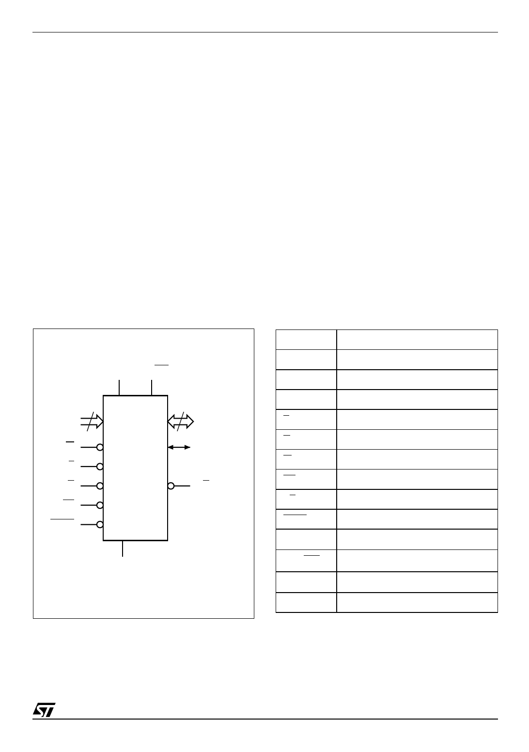
Figure 2. Logic Diagram
VCC VPP/WP
21
A0-A20
15
DQ0-DQ14
W
E
G
RP
BYTE
M29W320DT
M29W320DB
DQ15A–1
RB
VSS
AI90189B
Table 1. Signal Names
A0-A20
Address Inputs
DQ0-DQ7 Data Inputs/Outputs
DQ8-DQ14 Data Inputs/Outputs
DQ15A–1 Data Input/Output or Address Input
E
Chip Enable
G
Output Enable
W
Write Enable
RP
Reset/Block Temporary Unprotect
RB
Ready/Busy Output
BYTE
Byte/Word Organization Select
VCC
Supply Voltage
VPP/WP
VPP/Write Protect
VSS
Ground
NC
Not Connected Internally
5/44
Share Link: 