MAX3266EVKIT-SO 데이터 시트보기 (PDF) - Maxim Integrated
부품명
상세내역
제조사
MAX3266EVKIT-SO Datasheet PDF : 5 Pages
| |||
MAX3266/MAX3267 Evaluation Kits
To allow characterization without a photodiode, the
MAX3266 EV kit provides a simple circuit that emulates
a photodiode using common voltage output signal
sources.
The connector at INPUT is terminated with 50Ω to
ground. This voltage is then AC coupled to a resistance
in series with the MAX3266’s input, creating an input
current. U2 and U3 form a simple DC current source
that is used to apply a DC current to the input signal.
The values of the series resistive elements, R1 and R2,
have been carefully selected not to change the band-
width of the transimpedance amplifier. Surface-mount
resistors have parasitic capacitance that reduces their
impedance at frequencies above 1GHz. The user
should carefully evaluate any changes to R1 and R2
using the calibration network provided on the EV kit.
Table 1 shows the recommended resistor values.
Photodiode Emulation
The following procedure can be used to emulate the
high-speed current signal generated by a photodiode:
1) Select the desired optical power (PAVG in dBm)
and extinction ratio (re).
2) Calculate the average current (IAVG), and adjust R7
and R5 to obtain it.
IAVG
=
10(PAVG/10) ρ
1000
(ρ = photodiode responsivity in A/W)
3) Calculate the AC signal current, and adjust the sig-
nal generator to obtain it.
IINPUT = 2 ✕ IAVG(re - 1) / (re + 1)
For example:
1) Emulate a signal with an average power of -20dBm
and an extinction ratio of 10.
2) -20dBm optical power will produce 10µA of aver-
age input current (assume photodiode responsivity
of 1A/W). Install a current meter at JU1. Adjust R7
and R5 until the current is 10µA.
3) The signal amplitude is 2PAVG(re - 1) / (re + 1) =
16µA. To generate this current through the 1500Ω
input resistors, set the signal source to produce an
output level of 16µA ✕ 1500Ω = 24mVp-p.
Noise Measurement
Remove R2 before attempting noise measurements to
minimize input capacitance. With R2 removed the total
capacitance at the IN pin is approximately 0.5pF. Refer
to the Layout Considerations section in the MAX3266/
MAX3267 data sheet for more information.
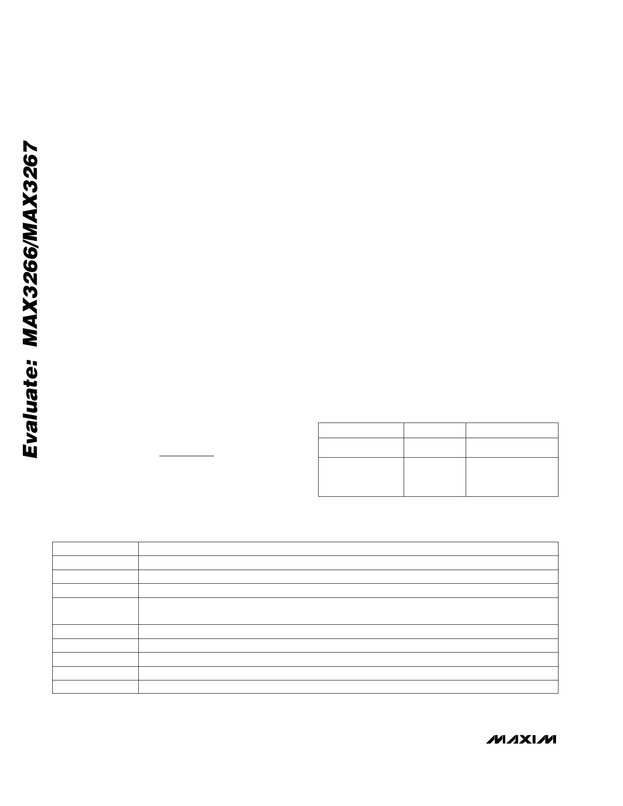
Table 1. Recommended Resistor Values
EVALUATION KIT
R1, R9
R2, R10
MAX3266EVKIT-SO 1000Ω (0603)
510Ω (0603)
MAX3267EVKIT-SO 200Ω (0402)
1020Ω (composed
of two 510Ω (0402)
resistors)
Table 2. Connections, Adjustments, and Control
CONTROL
VCC
+15V
GND
DESCRIPTION
Supply Voltage Connection (3.0 to 5.5V, 100mA current limit)
Supply Voltage Connection for Photodiode Emulator Circuit (+15V, 25mA)
Connection for Ground
JU1
When shunted, the photodiode emulation circuit is active. This is a convenient location to measure
the emulated photodiode current.
JU2
R5
R7
OUT+, OUT-
INPUT
Test Pin. Shunting JU2 disables the MAX3266/MAX3267 DC cancellation amplifier.
Potentiometer. Fine adjustment of the DC current input.
Potentiometer. Coarse adjustment of the DC current input.
Connections for the MAX3266/MAX3267 Output Signal
Input Connection for a Signal Generator
2 _______________________________________________________________________________________
Share Link: 