NX3V1T66_08 데이터 시트보기 (PDF) - NXP Semiconductors.
부품명
상세내역
제조사
NX3V1T66_08 Datasheet PDF : 18 Pages
| |||
NXP Semiconductors
NX3V1T66
Low-voltage analog switch
Table 8. Resistance RON …continued
At recommended operating conditions; voltages are referenced to GND (ground = 0 V); for graphs see Figure 8 to Figure 13.
Symbol Parameter
Conditions
Tamb = −40 °C to +85 Tamb = −40 °C to +125 °C Unit
°C
Min Typ[1] Max
Min
Max
RON(flat)
ON resistance
(flatness)
VI = GND to VCC;
ISW = 100 mA
VCC = 1.4 V
VCC = 1.65 V
VCC = 2.3 V
VCC = 2.7 V
[2]
-
0.5 1.7
-
-
0.25 0.6
-
-
0.1 0.2
-
-
0.1 0.2
-
1.8
Ω
0.7
Ω
0.2
Ω
0.2
Ω
[1] Typical values are measured at Tamb = 25 °C.
[2] Flatness is defined as the difference between the maximum and minimum value of ON resistance measured at identical VCC and
temperature.
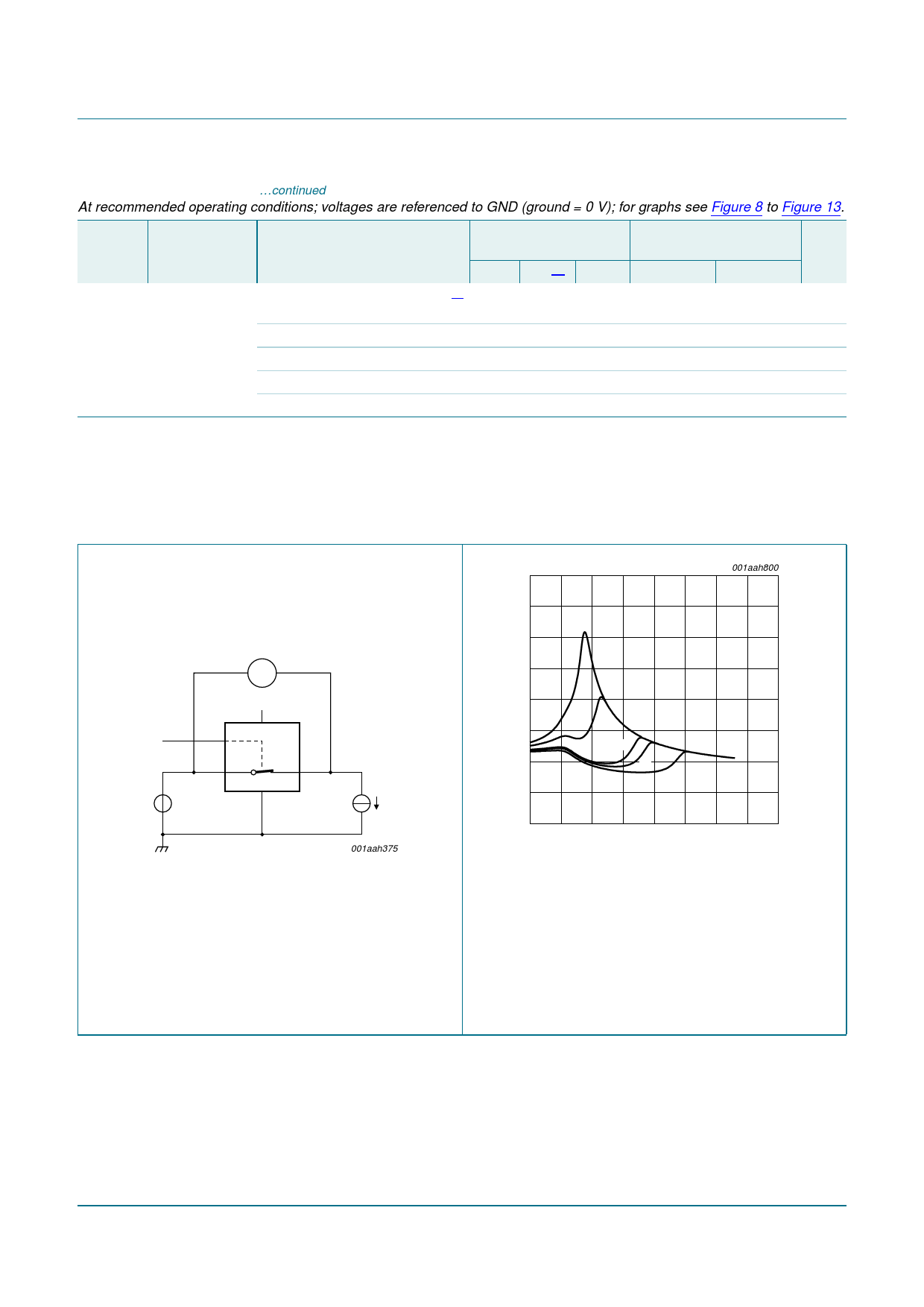
11.3 ON resistance test circuit and graphs
VSW
VCC
VIH
E
Z
Y
VI
GND
RON = VSW / ISW.
ISW
001aah375
Fig 7. Test circuit for measuring ON resistance
0.8
RON
(Ω)
0.6
001aah800
(1)
0.4
(2)
(3)
0.2
(4)
(5)
0
0
1
2
3
4
VI (V)
(1) VCC = 1.5 V.
(2) VCC = 1.8 V.
(3) VCC = 2.5 V.
(4) VCC = 2.7 V.
(5) VCC = 3.3 V.
Measured at Tamb = 25 °C.
Fig 8. Typical ON resistance as a function of input
voltage
NX3V1T66_2
Product data sheet
Rev. 02 — 24 July 2008
© NXP B.V. 2008. All rights reserved.
6 of 18
Share Link: 