FDC2512 데이터 시트보기 (PDF) - KEXIN Industrial
부품명
상세내역
제조사
FDC2512 Datasheet PDF : 4 Pages
| |||
SMD Type
MOSFET
N-Channel Enhancement MOSFET
FDC2512 (KDC2512)
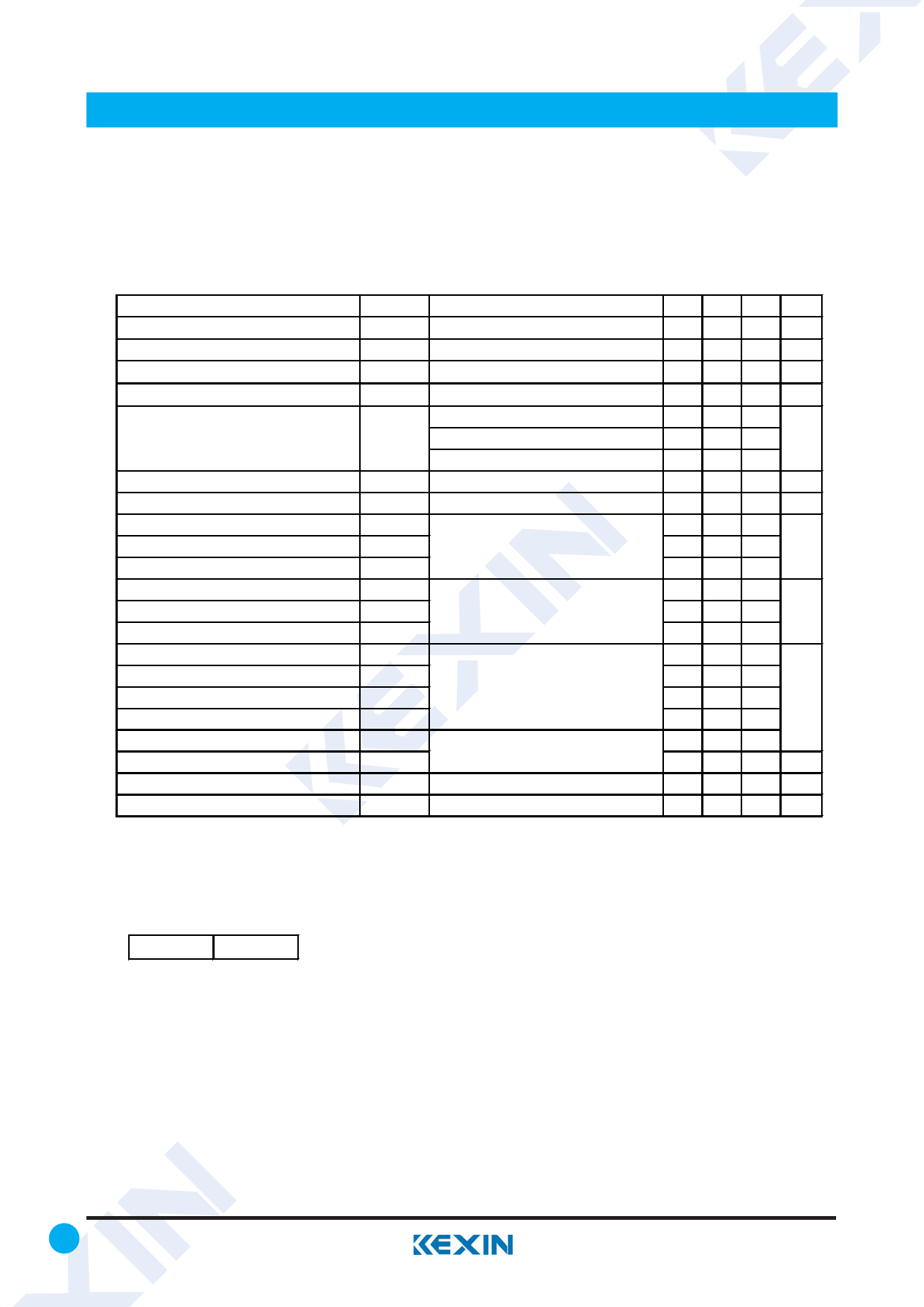
■ Electrical Characteristics Ta = 25℃
Parameter
Drain-Source Breakdown Voltage
Zero Gate Voltage Drain Current
Gate-Body Leakage Current
Gate Threshold Voltage *1
Static Drain-Source On-Resistance *1
On State Drain Current *1
Forward Transconductance *1
Input Capacitance
Output Capacitance
Reverse Transfer Capacitance
Total Gate Charge
Gate Source Charge
Gate Drain Charge
Turn-On DelayTime
Turn-On Rise Time
Turn-Off DelayTime
Turn-Off Fall Time
Body Diode Reverse Recovery Time
Body Diode Reverse Recovery Charge
Maximum Body-Diode Continuous Current
Diode Forward Voltage *1
Symbol
VDSS
IDSS
IGSSF
VGS(th)
RDS(On)
ID(ON)
gFS
Ciss
Coss
Crss
Qg
Qgs
Qgd
td(on)
tr
td(off)
tf
trr
Qrr
IS
VSD
Test Conditions
ID=250μA, VGS=0V
VDS=120V, VGS=0V
VDS=0V, VGS=±20V
VDS=VGS , ID=250μA
VGS=10V, ID=1.4A
VGS=10V, ID=1.4A TJ=125℃
VGS=6.0V, ID=1.3A
VGS=10V, VDS=5V
VDS=10V, ID=1.4A
VGS=0V, VDS=75V, f=1MHz
VGS=10V, VDS=75V, ID=1.4A *1
VGS=10V, VDS=75V, ID=1A,RGEN=6Ω *1
IF= 1.4A, dI/dt= 300A/μs *1
IS=1.3A,VGS=0V
Min Typ Max Unit
150
V
1 μA
±100 nA
2 2.6 4
V
319 425
624 875 mΩ
332 475
4
A
4
S
344
22
pF
9
8 11
1.5
nC
2.3
6.5 13
3.5 7
22 33 ns
4
8
45.8
119
nC
1.3 A
0.8 1.2 V
*1 Pulse Test: Pulse Width < 300μs, Duty Cycle < 2.0%
■ Marking
Marking
2512
2 www.kexin.com.cn
Share Link: 