CMX605(1999) 데이터 시트보기 (PDF) - MX-COM Inc
부품명
상세내역
제조사
CMX605 Datasheet PDF : 22 Pages
| |||
Digital Line to POTS Interface
11
CMX605 Preliminary Information
4.8 ‘C-BUS’ Interface
This block provides for the transfer of data and control or status information between the CMX605’s internal
registers and the µC over the ‘C-BUS’ serial bus. Each 'C-BUS' transaction consists of a single Register
Address byte sent from the µC, as illustrated in Figure 4, which may then be followed by either of:
A single data byte sent from the µC to be written into one of the CMX605’s Write Only Registers, as
illustrated in Figure 5.
A single byte of data read out from one of the CMX605’s Read Only Registers, as illustrated in Figure 6.
Data sent from the µC on the Command Data (COMMAND DATA) line is clocked into the CMX605 on the
rising edge of the Serial Clock (SERIAL CLOCK) input. Reply Data (REPLY DATA) sent from the CMX605 to
the µC is valid when the Serial Clock is high. The interface is compatible with the most common µC serial
interfaces such as SCI, SPI and Microwire, and may also be easily implemented with general purpose µC I/O
pins controlled by a simple software routine. See Figure 9 for detailed ‘C-BUS’ timing requirements.
CS
SERIAL CLOCK
COMMAND DATA
REPLY DATA
765432 10
Address (01 Hex = Reset)
Hi-Z
Note:
The SERIAL CLOCK
line may be high or low at
the start and end of each
transaction.
= Level not important
Figure 4: ‘C-BUS’ Transactions (Single byte from µC)
CS
SERIAL CLOCK
COMMAND DATA
765432 10
Address
REPLY DATA Hi-Z
765432 10
Data to CMX605
Figure 5: ‘C-BUS’ Transactions (One Address and one Data Byte from µC)
CS
SERIAL CLOCK
COMMAND DATA
REPLY DATA
765432 10
Address
Hi-Z
765432 10
Data from CMX605
Figure 6: ‘C-BUS’ Transactions (One Address Byte from µC and one Reply Byte from CMX605)
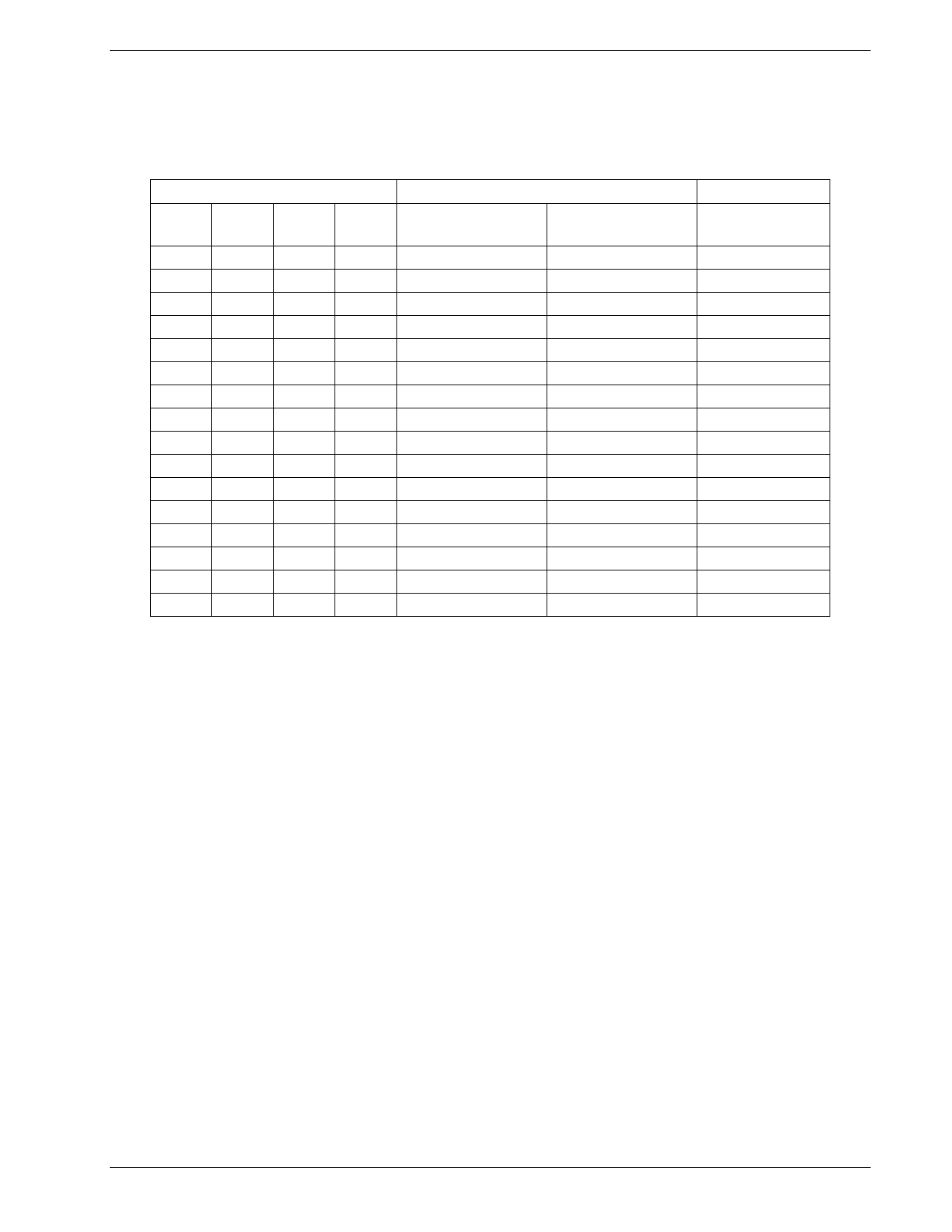
4.9 ‘C-BUS’ Registers
Addr
$01
$D0
Register
RESET
SETUP
$D1 MODE
$D3 TX DATA
$D4 TX TONES
7
N/A
Uncommitted
Amplifier
0 = Disable
1 = Enable
SPM Output:
0 = Disable
1 = Enable
D7
D7
6
N/A
Tx Enable:
0 = Disable
1 = Enable
Command Data Byte (Bits 7 – 0)
5
4
3
N/A
N/A
N/A
DTMF Rx: SPM: Reserved
0 = Disable 0 = 12kHz set to 0
1 = Enable 1 = 16kHz
2
N/A
Reserved
set to 0
1
N/A
FSK mode:
0 = Sync
1 = Async
0
N/A
FSK mode:
0 = V23
1 = Bell 202
Tone/FSK:
0 = Disable
1 = Enable
D6
D6
Tone/FSK:
0 = Tone
1 = FSK
D5
D5
Tx Level:
(MSB)
D4
D4
Tx Level:
D3
D3
Tx Level: Tone Fields: Tone Fields:
(LSB)
(MSB)
(LSB)
D2
D1
D0
D2
D1
D0
Table 10: Write Only Registers
©1999 MX-COM, Inc.
www.mxcom.com tel: 800 638 5577 336 744 5050 fax: 336 744 5054
Doc. # 20480195.003
4800 Bethania Station Road, Winston-Salem, NC 27105-1201 USA
All trademarks and service marks are held by their respective companies.
Share Link: 