74HC32-Q100 데이터 시트보기 (PDF) - NXP Semiconductors.
부품명
상세내역
제조사
74HC32-Q100 Datasheet PDF : 15 Pages
| |||
NXP Semiconductors
74HC32-Q100; 74HCT32-Q100
Quad 2-input OR gate
Table 7. Dynamic characteristics
GND = 0 V; CL = 50 pF; for load circuit see Figure 7.
Symbol Parameter
Conditions
Min
74HCT32-Q100
tpd
propagation delay nA, nB to nY; see Figure 6
VCC = 4.5 V
VCC = 5.0 V; CL = 15 pF
tt
transition time
VCC = 4.5 V; see Figure 6
CPD
power dissipation per package;
capacitance
VI = GND to VCC 1.5 V
[1]
-
-
[2]
-
[3]
-
[1] tpd is the same as tPHL and tPLH.
[2] tt is the same as tTHL and tTLH.
[3] CPD is used to determine the dynamic power dissipation (PD in W):
PD = CPD VCC2 fi N + (CL VCC2 fo) where:
fi = input frequency in MHz;
fo = output frequency in MHz;
CL = output load capacitance in pF;
VCC = supply voltage in V;
N = number of inputs switching;
(CL VCC2 fo) = sum of outputs.
25 C
Typ
11
9
7
28
40 C to +125 C Unit
Max Max
Max
(85 C) (125 C)
24
30
-
-
15
19
-
-
36 ns
- ns
22 ns
- pF
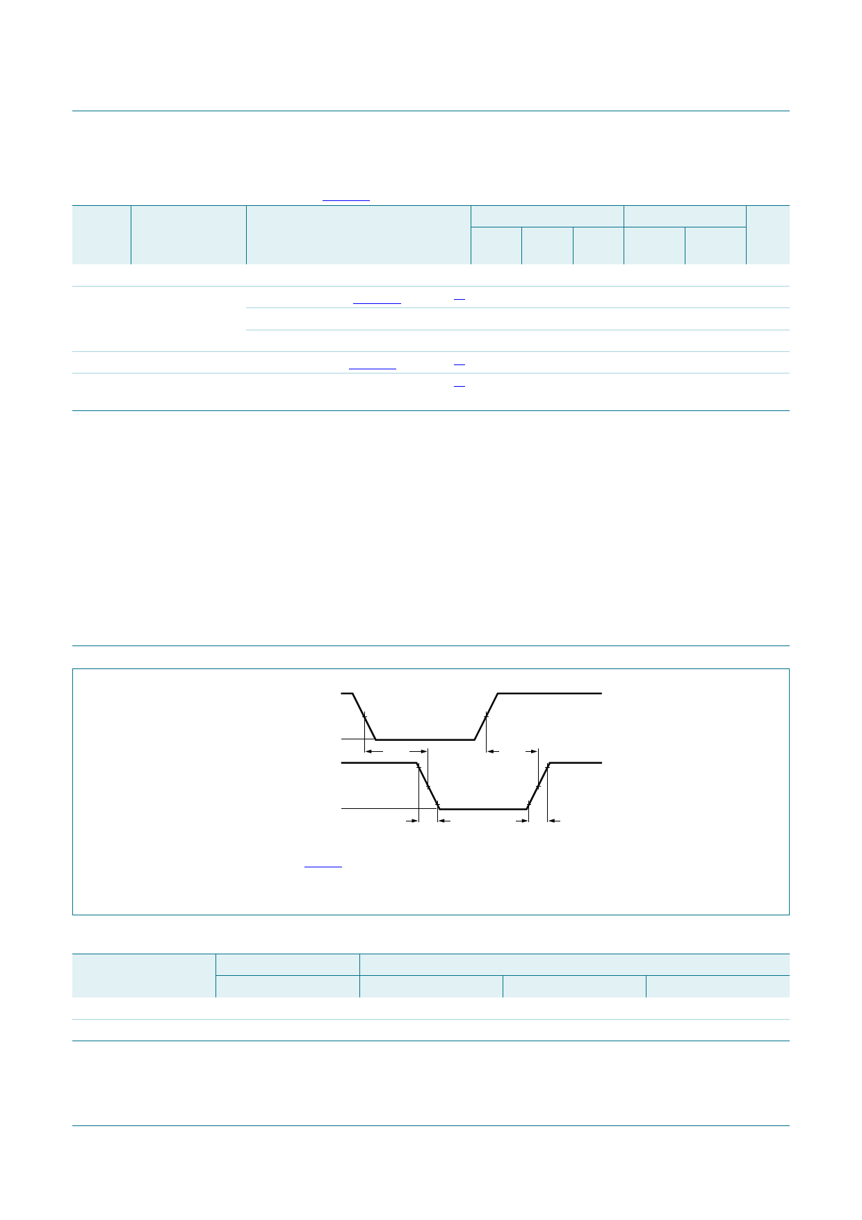
11. Waveforms
9,
Q$ Q% LQSXW
*1'
92+
Q< RXWSXW
92/
90
W3+/
9<
W7+/
90
9;
W3/+
W7/+
Fig 6.
Measurement points are given in Table 9.
VOL and VOH are typical output voltage levels that occur with the output load.
Input to output propagation delays
DDD
Table 8. Measurement points
Type
Input
74HC32-Q100
74HCT32-Q100
VM
0.5VCC
1.3 V
Output
VM
0.5VCC
1.3 V
VX
0.1VCC
0.1VCC
VY
0.9VCC
0.9VCC
74HC_HCT32_Q100
Product data sheet
All information provided in this document is subject to legal disclaimers.
Rev. 1 — 1 August 2012
© NXP B.V. 2012. All rights reserved.
7 of 15
Share Link: 