CAT25010Y 데이터 시트보기 (PDF) - Catalyst Semiconductor => Onsemi
부품명
상세내역
제조사
CAT25010Y Datasheet PDF : 11 Pages
| |||
CAT25010/20/40
array because the write enable latch will not have been
properly set. Also, for a successful write operation the
address of the memory location(s) to be programmed
must be outside the protected address field location
selected by the block protection level.
Byte Write
Once the device is in a Write Enable state, the user may
proceed with a write sequence by setting the CS low,
issuing a write instruction via the SI line, followed by the
8-bit address for 25010/20/40 (for the 25040, bit 3 of the
read data instruction contains address A8). Programming
will start after the CS is brought high. Figure 6 illustrates
byte write sequence.
During an internal write cycle, all commands will be
ignored except the RDSR (Read Status Register)
instruction.
The Status Register can be read to determine if the write
cycle is still in progress. If Bit 0 of the Status Register is
set at 1, write cycle is in progress. If Bit 0 is set at 0, the
device is ready for the next instruction
Page Write
The CAT25010/20/40 features page write capability.
After the initial byte, the host may continue to write up to
16 bytes of data to the CAT25010/20/40. After each
byte of data received, lower order address bits are
internally incremented by one; the high order bits of
address will remain constant. The only restriction is that
the X (X=16 for CAT25010/20/40) bytes must reside on
the same page. If the address counter reaches the end
of the page and clock continues, the counter will “roll
over” to the first address of the page and overwrite any
data that may have been written. The CAT25010/20/40
is automatically returned to the write disable state at the
completion of the write cycle. Figure 8 illustrates the
page write sequence.
To write to the status register, the WRSR instruction
should be sent. Only Bit 2 and Bit 3 of the status register
can be written using the WRSR instruction. Figure 7
illustrates the sequence of writing to status register.
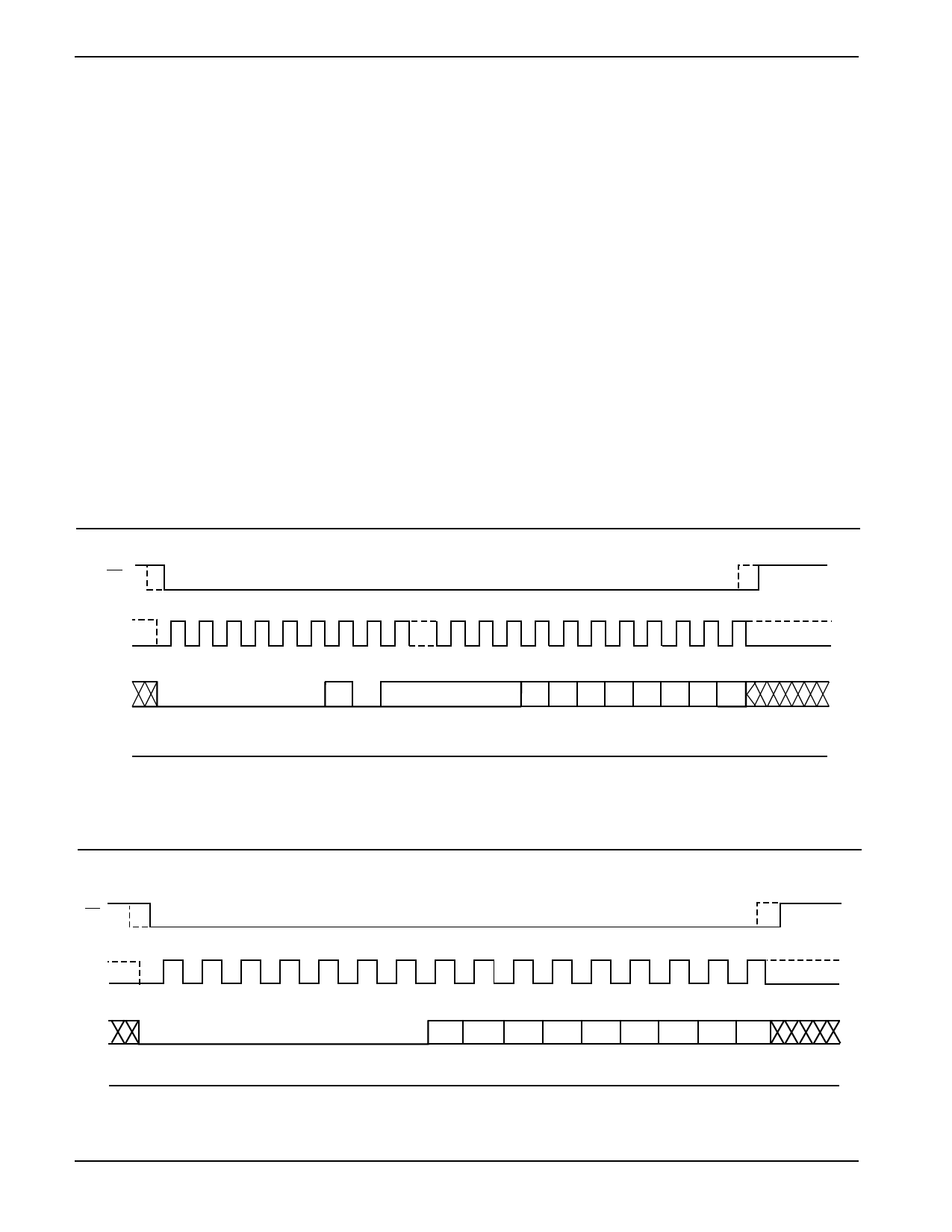
Figure 6. Write Instruction Timing
CS
012345678
21 22 23 24 25 26 27 28 29 30 31
SK
OPCODE
SI
00 00 00 10
ADDRESS
DATA IN
D7 D6 D5 D4 D3 D2 D1 D0
SO
HIGH IMPEDANCE
Note: Dashed Line= mode (1, 1) – – – – –
*X=0 for 25010, 25020 ; X=A8 for 25040
Figure 7. WRSR Timing
CS
SCK
0
1
2
3
4
5
6
7
8
9 10 11 12 13 14 15
OPCODE
DATA IN
SI
0
0
0
0
00
0
1
7
6
5
4
3
2
10
MSB
SO
HIGH IMPEDANCE
Note: Dashed Line= mode (1, 1) – – – – –
Doc. No. 1006, Rev. L
8
Share Link: 