MPS-U55 데이터 시트보기 (PDF) - New Jersey Semiconductor
부품명
상세내역
제조사
MPS-U55 Datasheet PDF : 2 Pages
| |||
<Se.mi-C.onauck.oi iJ-ioducti, One,
20 STERN AVE.
SPRINGFIELD, NEW JERSEY 07081
U.S.A.
MPS-U55, MPS-U56 (continued)
TELEPHONE: (201) 376-2922
(212)227-6005
FAX; (201) 376-8960
ELECTRICAL CHARACTERISTICS <TA - 25°C unless otherwise noted)
Characteristic
Symbol
Typ
OFF CHARACTERISTICS
Collector-Emitter Breakdown Voltage
(lc- I.OmAdc, IB -01
Emitter-Base Breakdown Voltage
(IE- 100»iAde, lc-0)
Collector Cutoff Current
(VCB-40Vdc, le -0)
(VCB-60Vdc, IE -01
BVcEO
MPS-U55
60
-
—
MPS-U56
80
-
-
8VEBO
4.0
-
-
ICBO
MPS-U5S
-
MPS-U56
-
—
100
-
100
ON CHARACTERISTICS
DC Current Gain ( 1 )
dc " 50 mAdc, VCE • '-0 Vdc)
Uc • 250 mAdc, VCE • 1-0 Vdc)
( 1 C • 500 mAdc, VCE " 1 -0 Vdc)
Collector-Emitter Saturation Voltage! 1)
(1C * 250 mAdc, IB - 10 mAdc)
dC " 250 mAdc, IB - 25 mAdc)
Base-Emitter On Voltage 11)
(1C • 250 mAdc, VCE " 5.0 Vdc)
SMALL-SIGNAL CHARACTERISTICS
Current-Gain— Bandwidth Product
dC - 200 mAdc. VCE " 5.0 Vdc, f - 100 MHz)
Output Capacitance
<VCB • 10 vdc- IE • ". * • 100 kHz)
(l)Pulu Test: Pulu Width £300 I". Duty Cycle
"FE
80
160
-
50
130
-
-
80
-
VcE(sat)
-
0.22
0.5
-
0.1S
-
vBE(on)
-
0.78
1.2
«T
SO
100
-
Cob
"
10
15
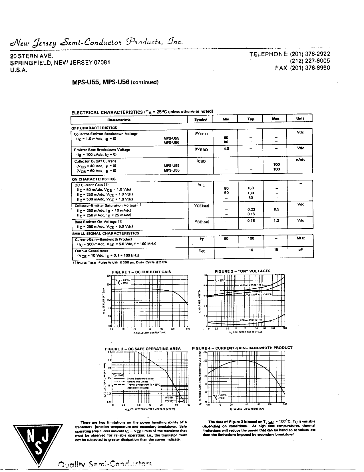
FIGURE 1 - DC CURRENT GAIN
11
-•vc
j • li' e"
" •
"S N
\
FIGURE 2 - "ON" VOLTAGES
10
20
Unit
Vdc
Vdc
nAdc
-
Vdc
Vdc
MHz
pF
50
100
20
1C. COLLECTOR CURRENT (mA)
10 2.0
50
10 20
SO 100 200
5QO
LC, COLLECTOR CURRENT (mA)
FIGURE 3 - DC SAFE OPERATINGAREA
FIGURE 4 - CURRENT-GAIN-BANDWIDTH PRODUCT
1.0
fc
I OS
ss
:
^r
Tj - 1M"C
02
n--
01
-
J
0• 011 0
20
cond Bfiikdown imnttf
80ndirwjWwt Limn id
ThKirnl Limitmon 9 Tc • 25'C
AHifilmbli To BVCE0
1 HH-T-H
SO
10
20
s
\s
V
MP q
MPSU5 s- ^5"
SO
10( 0
Vet, COLLECTOR EMITTER VOLTAGE (VOLTS)
B
S
IX
i 100
*
*?
s
vrf S O V d c
7
t 50
JM5°C
ID
1 <)
"•• \
V
\S .
>
S0
00
2»
so
There ere two limitation! on the power handling ability of a
transinor: junction temperature and secondary breakdown. Safe
operating area curves indicate Ic - VCE limits of the tramittor that
must be observed for reliable operation: i.e.. the transistor must
not be subjected to greater dissipation than the curves indicate.
The data of Figure 3 is bawd on Tj(p|(| - 150°C. TC is variable
depending on conditions. At high caw temperatures, thermal
limitations will reduce the power that can be handled to values less
than the limitations impend by secondary breakdown
Ouaiitv S
Share Link: 