TCM680 데이터 시트보기 (PDF) - Microchip Technology
부품명
상세내역
제조사
TCM680 Datasheet PDF : 18 Pages
| |||
TCM680
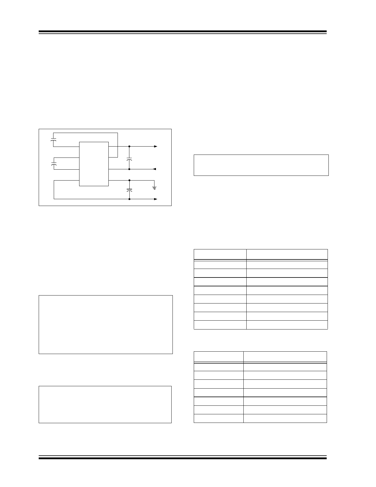
5.0 APPLICATIONS INFORMATION
5.1 Voltage Multiplication and
Inversion
The TCM680 performs voltage multiplication and inver-
sion simultaneously, providing positive and negative
outputs (Figure 5-1). The magnitude of both outputs is,
approximately, twice the input voltage. Unlike other
switched capacitor converters, the TCM680 requires
only four external capacitors to provide both functions
simultaneously.
C1 +
22 µF
C2 +
22 µF
1 C1- VOUT+ 8
2 C2+
C1+ 7
3
TCM680
C2-
VIN
6
4 VOUT- GND 5
+ C4
22 µF
+ C3
22 µF
VOUT+
VIN
GND
VOUT-
FIGURE 5-1:
Converter.
Positive and Negative
5.2 Capacitor Selection
The TCM680 requires only 4 external capacitors for
operation, which can be inexpensive, polarized alumi-
num electrolytic types. For the circuit in Figure 5-1, the
output characteristics are largely determined by the
external capacitors. An expression for ROUT can be
derived as shown below:
EQUATION
ROUT+ = 4(RSW1 + RSW2 + ESRC1 + RSW3 + RSW4 + ESRC2)
+4(RSW1 + RSW2 + ESRC1 + RSW3 + RSW4 + ESRC2)
+1/(fPUMP x C1) + 1/(fPUMP x C2) + ESRC4
ROUT– = 4(RSW1 + RSW2 + ESRC1 + RSW3 + RSW4 + ESRC2)
+4(RSW1 + RSW2 + ESRC1 + RSW3 + RSW4 + ESRC2)
+1/(fPUMP x C1) + 1/(fPUMP x C2) + ESRC3
Assuming all switch resistances are approximately
equal:
EQUATION
ROUT+ = 32RSW + 8ESRC1 + 8ESRC2 + ESRC4
+1/(fPUMP x C1) + 1/(fPUMP x C2)
ROUT– = 32RSW + 8ESRC1 + 8ESRC2 + ESRC3
+1/(fPUMP x C1) + 1/(fPUMP x C2)
ROUT is typically 140Ω at +25°C with VIN = +5V and C1
and C2 as 4.7 µF low ESR capacitors. The fixed term
(32RSW) is about 130Ω. It can easily be seen that
increasing or decreasing values of C1 and C2 will affect
efficiency by changing ROUT. However, be careful
about ESR. This term can quickly become dominant
with large electrolytic capacitors. Table 5-1 shows
ROUT for various values of C1 and C2 (assume 0.5Ω
ESR). C1 and C4 must be rated at 6 VDC or greater
while C2 and C3 must be rated at 12 VDC or greater.
Output voltage ripple is affected by C3 and C4.
Typically, the larger the value of C3 and C4, the less the
ripple for a given load current. The formula for
VRIPPLE(p-p) is given below:
EQUATION
VRIPPLE(p-p)+ = {1/[2(fPUMP /3) x C4] + 2(ESRC4)} (IOUT+)
VRIPPLE(p-p)– = {1/[2(fPUMP /3) x C3] + 2(ESRC3)} (IOUT–)
For a 10 µF (0.5Ω ESR) capacitor for C3, C4,
fPUMP = 21 kHz and IOUT = 10 mA, the peak-to-peak
ripple voltage at the output will be less than 100 mV. In
most applications (IOUT ≤ 10 mA), 10-20 µF output
capacitors and 1-5 µF pump capacitors will suffice.
Table 5-2 shows VRIPPLE for different values of C3 and
C4 (assume 1 Ω ESR).
TABLE 5-1: OUTPUT RESISTANCE
VS. C1, C2
C1, C2 (µF)
ROUT+, ROUT- (Ω)
0.1
1089
0.47
339
1
232
3.3
165
4.7
157
10
146
22
141
100
137
TABLE 5-2:
C3, C4 (µF)
VRIPPLE PEAK-TO-PEAK
VS. C3, C4 (IOUT 10 mA)
VRIPPLE(p-p)+,VRIPPLE(p-p)- (mV)
0.47
1540
1
734
3.3
236
4.7
172
10
91
22
52
100
27
DS21486C-page 8
© 2005 Microchip Technology Inc.
Share Link: 