R3111D501C-TR-F 데이터 시트보기 (PDF) - RICOH Co.,Ltd.
부품명
상세내역
제조사
R3111D501C-TR-F Datasheet PDF : 44 Pages
| |||
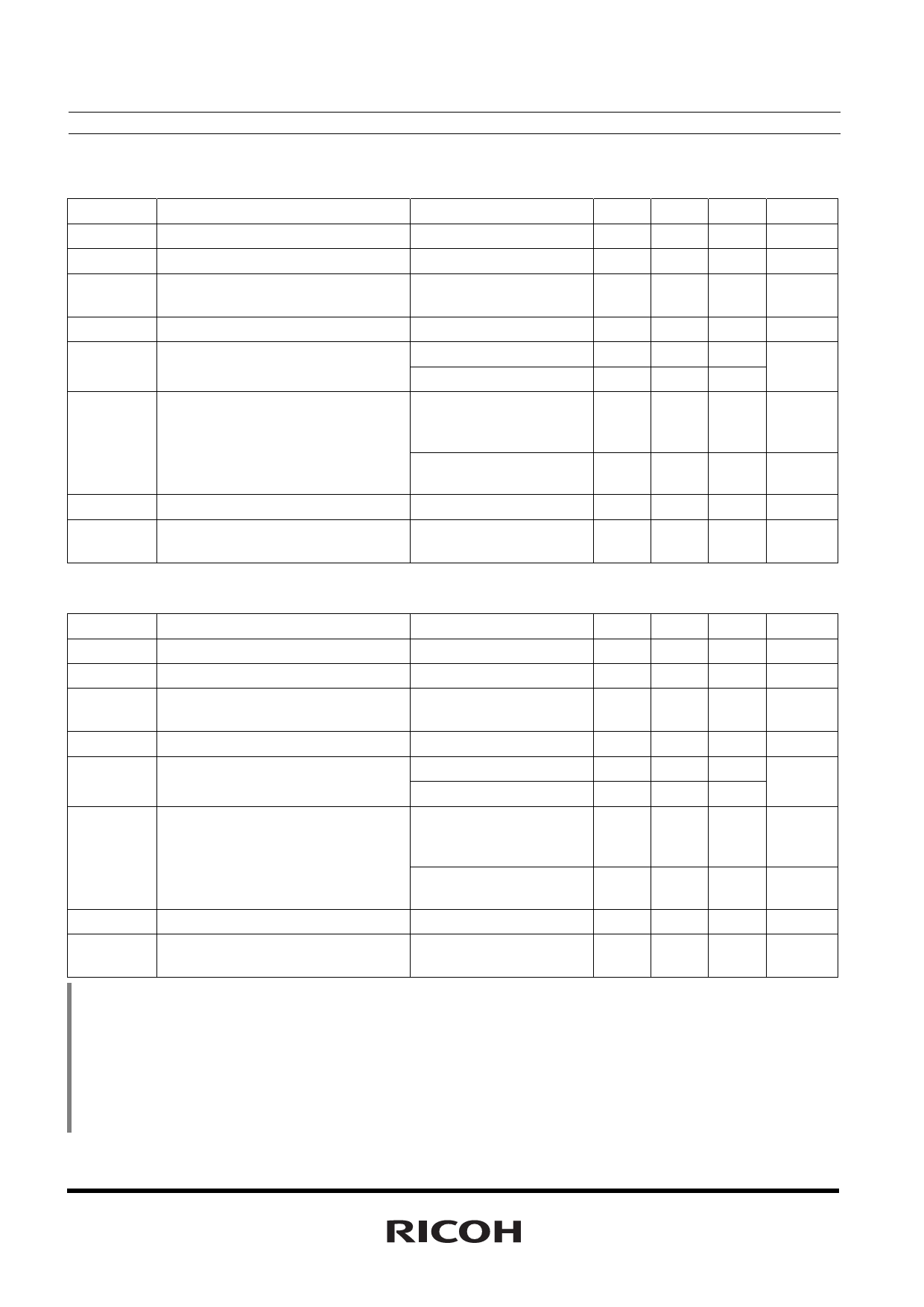
R3111x
• R3111x45xA/C
Symbol
−VDET
VHYS
ISS
VDDH
VDDL
IOUT
tPLH
∆−VDET/
∆Topt
Item
Detector Threshold
Detector Threshold Hysteresis
Supply Current
Maximum Operating Voltage
Minimum Operating Voltage∗Note1
Output Current (Driver Output Pin)
Output Delay Time∗Note2
Detector Threshold Temperature
Coefficient
Conditions
VDD=4.34V
VDD=6.50V
Topt=25°C
−40°C <= Topt <= 85°C
Nch
VDS=0.05V, VDD=0.70V
VDS=0.50V, VDD=1.50V
Pch
VDS=−2.1V,VDD=8.0V
−40°C <= Topt <= 85°C
Topt=25°C
Min. Typ. Max. Unit
4.410 4.500 4.590
V
0.135 0.225 0.315
V
1.1 3.3
1.3 3.9
µA
10
V
0.55 0.70
V
0.65 0.80
0.01 0.05
mA
1.00 2.00
1.5 3.0
mA
100
µs
±100
ppm/°C
• R3111x54xA/C
Topt=25°C
Symbol
−VDET
VHYS
ISS
VDDH
VDDL
IOUT
tPLH
∆−VDET/
∆Topt
Item
Detector Threshold
Detector Threshold Hysteresis
Supply Current
Maximum Operating Voltage
Minimum Operating Voltage∗Note1
Output Current
(Driver Output Pin)
Output Delay Time∗Note2
Detector Threshold Temperature
Coefficient
Conditions
VDD=5.20V
VDD=7.40V
Topt=25°C
−40°C <= Topt <= 85°C
Nch
VDS=0.05V, VDD=0.70V
VDS=0.50V, VDD=1.50V
Pch
VDS=−2.1V, VDD=8.0V
−40°C <= Topt <= 85°C
Min. Typ. Max. Unit
5.292 5.400 5.508
V
0.162 0.270 0.378
V
1.2 3.6
1.4 4.2
µA
10
V
0.55 0.70
V
0.65 0.80
0.01 0.05
mA
1.00 2.00
1.5 3.0
mA
100
µs
±100
ppm/°C
∗Note1: Minimum operating voltage means the value of input voltage when output voltage maintains 0.1V or less. (In
the case of Nch Open Drain Output type, the output pin is pulled up with a resistance of 470kΩ to 5.0V.)
∗Note2: In the case of CMOS Output type: The time interval between the rising edge of VDD input pulse from 0.7V
to (+VDET)+2.0V and output voltage level becoming to ((+VDET)+2.0V)/2.
In the case of Nch Open Drain Output type: The output pin is pulled up with a resistance of 470kΩ to
5.0V, the time interval between the rising edge of VDD input pulse from 0.7V to (+VDET)+2.0V and output
voltage level becoming to 2.5V.
8
Share Link: 