LHF16KA7 데이터 시트보기 (PDF) - Sharp Electronics
부품명
상세내역
제조사
LHF16KA7 Datasheet PDF : 53 Pages
| |||
_-
LHFlGKA7
8
I
--
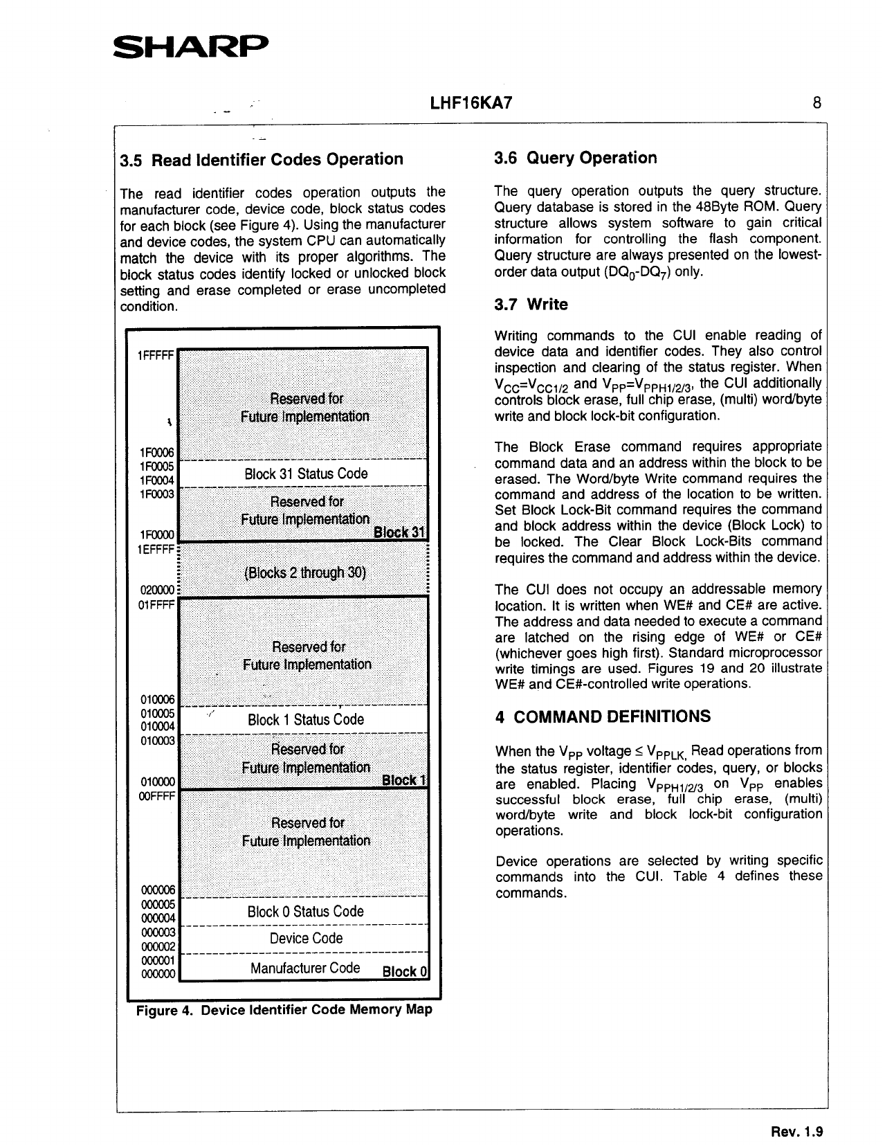
3.5 Read Identifier Codes Operation
3.6 Query Operation
The read identifier codes operation outputs the
manufacturer code, device code, block status codes
for each block (see Figure 4). Using the manufacturer
and device codes, the system CPU can automatically
match the device with its proper algorithms. The
block status codes identify locked or unlocked block
setting and erase completed or erase uncompleted
condition.
The query operation outputs the query structure.
Query database is stored in the 48Byte ROM. Query
structure allows system software to gain critical
information for controlling the flash component.
Query structure are always presented on the lowest-
order data output (DQc-DQ,) only.
3.7 Write
1FFFFF :.. :
..:,>...A., ..
1;;
':.. .:
,,...
,;.' . . .,.
'. .' j.: R&&&&,
.,:,': .:' .:
l !:;"'..,.
,:
:. .
Future
;.
~+irnentatt~n
'.
,Fm;
..
:.
,K)oo5 iilr-' l_l..d+ - -----------_-------1----
,IFF0o0o0o43 T---,-. ~____B_lock--;31_S__ta_tTu-s--C--o--dye---I
JGxwv~d for
;.
,Foooo :,.., :‘i:
tfutye h: $e.merrtiian B&;k31
IEFFFF;:. :' . ; : ':,,..
02oooo;:mw:.. ... ,+
::
: . '(~ioiks2thi~gl-l~)
..:
,, '.', :
.,.
;
:.
OlFFFF ', " : ..,I. ; ,:" "')
o0011,o0o0(oy0o4&5(l-I_-_-”l_-l_.-/_-’-_l-_~_-_-_l’B_l-ll-o--y--c.-,k-_rl1_l-_-S_-tl_lal_-tul---s---_-C-_-o---d---e-------
010003-
.. .. i&e&ed~for
,:
: .; :...:.f;uture:‘tmplemen~tiQn
..
01~ 1. .,: .’ ‘.,
Block”
OOFFFF ;. 1.
Resewed far
Future Implementation
ooooO6_. __--- ____-- ____--------_------ ------
coo005
OoOcQ4
_____-_____B-l_o_c_k_0__S_t-a--tu--s---C--o-d--e-----
OOooOOoamQnOI3o21___________M_a_n_Du_ef_av_cic_tue_r_eC-r-o-d-C-e-o--d-e--------Block (
Writing commands to the CUI enable reading of
device data and identifier codes. They also control
inspection and clearing of the status register. When
Vcc=Vcc1,2 and VPP=VPPHt/2/3, the CUI additionally
controls block erase, full chip erase, (multi) wordlbyte
write and block lock-bit configuration.
The Block Erase command requires appropriate
command data and an address within the block to be
erased. The Word/byte Write command requires the
command and address of the location to be written.
Set Block Lock-Bit command requires the command
and block address within the device (Block Lock) to
be locked. The Clear Block Lock-Bits command
requires the command and address within the device.
The CUI does not occupy an addressable memory
location. It is written when WE# and CE# are active.
The address and data needed to execute a command
are latched on the rising edge of WE# or CE#
(whichever goes high first). Standard microprocessor
write timings are used. Figures 19 and 20 illustrate
WE# and CE#-controlled write operations.
4 COMMAND DEFINITIONS
When the V,, voltage I V,,,,, Read operations from
the status register, identifier codes, query, or blocks
are enabled. Placing V,,,,,us on V,, enables
successful block erase, full chip erase, (multi)
word/byte write and block lock-bit configuration
operations.
Device operations are selected by writing specific
commands into the CUI. Table 4 defines these
commands.
Figure 4. Device Identifier Code Memory Map
Rev. 1.9
Share Link: 