CDP68HC68T1 데이터 시트보기 (PDF) - Renesas Electronics
부품명
상세내역
제조사
CDP68HC68T1 Datasheet PDF : 24 Pages
| |||
CDP68HC68T1
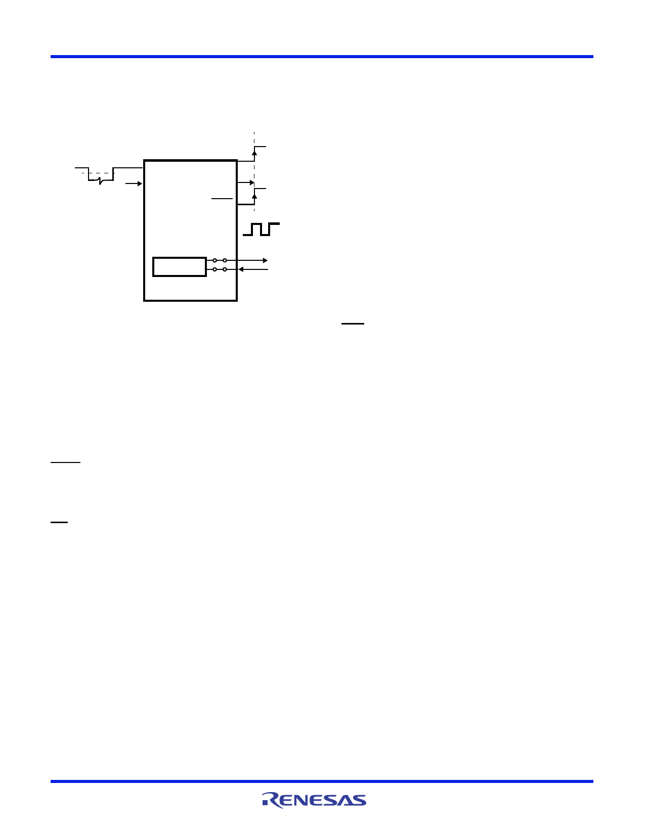
2. The second condition that releases Power-Down occurs
when the level on the VSYS pin rises about 1.0V above
the level at the VBATT input, after previously falling to the
level of VBATT (see Figure 6) in the Battery Backup Mode
or VSYS falls to logic low and returns high in the Single
Supply Mode.
VBATT
VSYS
PSE
CPUR
CLK
OUT
SERIAL
INTERFACE
REAL-TIME CLOCK
CDP68HC68T1
MISO
MOSI
FIGURE 6. POWER-UP FUNCTIONAL DIAGRAM (INITIATED
BY A RISE IN VOLTAGE ON THE “VSYS” PIN)
CLK OUT
Clock output pin. One of seven frequencies can be selected
(or this output can be set low) by the levels of the three
LSB’s in the Clock-Control Register. If a frequency is
selected, it will toggle with a 50% duty cycle except 2Hz in
the 50Hz time base mode. (e.g. if 1Hz is selected, the output
will be high for 500ms and low for the same period). During
power-down operation (Bit 6 in Interrupt Control Register is
set to “1”), the clock-output pin will be set low.
CPUR
CPU reset output pin. This pin functions as an N-Channel
only, open-drain output and requires an external pull-up
resistor.
INT
Interrupt output pin. This output is driven from a single NFET
pulldown transistor and must be tied to an external pull-up
resistor. The output is activated to a low level when:
1. Power-sense operation is selected (B5 = 1 in Interrupt
Control Register) and a power failure occurs.
2. A previously set alarm time occurs. The alarm bit in the
Status Register and interrupt-out signal are delayed
30.5µs when 32kHz operation is selected and 15.3µs for
2MHz and 7.6µs for 4MHz.
3. A previously selected periodic interrupt signal activates.
The Status Register must be read to set the Interrupt output
high after the selected periodic interval occurs. This is also
true when conditions 1 and 2 activate the interrupt. If
power-down had been previously selected, the interrupt will
also reset the power-down functions.
SCK, MOSI, MISO
See “Serial Peripheral Interface (SPI)” on page 8.
CE
A positive chip-enable input. A low level at this input holds
the serial interface logic in a reset state. This pin is also used
for the watchdog function.
VSS
The negative power-supply pin that is connected to ground.
PSE
Power-supply enable output pin. This pin is used to control
power to the system. The pin is set high when:
1. VSYS rises above the VBATT voltage after VSYS was
placed low by a system failure.
2. An interrupt occurs.
3. A power-on reset (if VSYS is a logic high).
The PSE pin is set low by writing a high into bit 6
(power-down bit) in the Interrupt Control Register.
POR
Power-on reset. A Schmitt-trigger input that generates a
power-on internal reset signal using an external RC
network. Both control registers and frequency dividers for
the oscillator and line input are reset. The Status Register
is reset except for the first time up bit (B4), which is set.
Single supply or battery backup operation is selected at the
end of POR.
LINE
This input is used for two functions. When not used it
should be connected to VDD via a 10k resistor. The first
function utilizes the input signal as the frequency source for
the timekeeping counters. This function is selected by
setting Bit 6 in the Clock Control Register. The second
function enables the line input to sense a power failure.
Threshold detectors operating above and below VDD sense
an AC voltage loss. Bit 5 must be set to “1” in the Interrupt
Control Register and crystal or external clock source
operation is required. Bit 6 in the Clock Control Register
must be low to select XTAL operation.
Oscillator Circuit
The CDP68HC68T1 has an on-board 150k resistor that is
switched in series with its internal inverter when 32kHz is
selected via the Clock Control Register. Note: When first
powered up the series resistor is not part of the oscillator
circuit. (The CDP68HC68T1 sets up for a 4MHz oscillator).
FN1547 Rev 9.00
Decemember 8, 2015
Page 10 of 24
Share Link: 