MJE5740 데이터 시트보기 (PDF) - Motorola => Freescale
부품명
상세내역
제조사
MJE5740 Datasheet PDF : 6 Pages
| |||
MJE5740 MJE5741 MJE5742
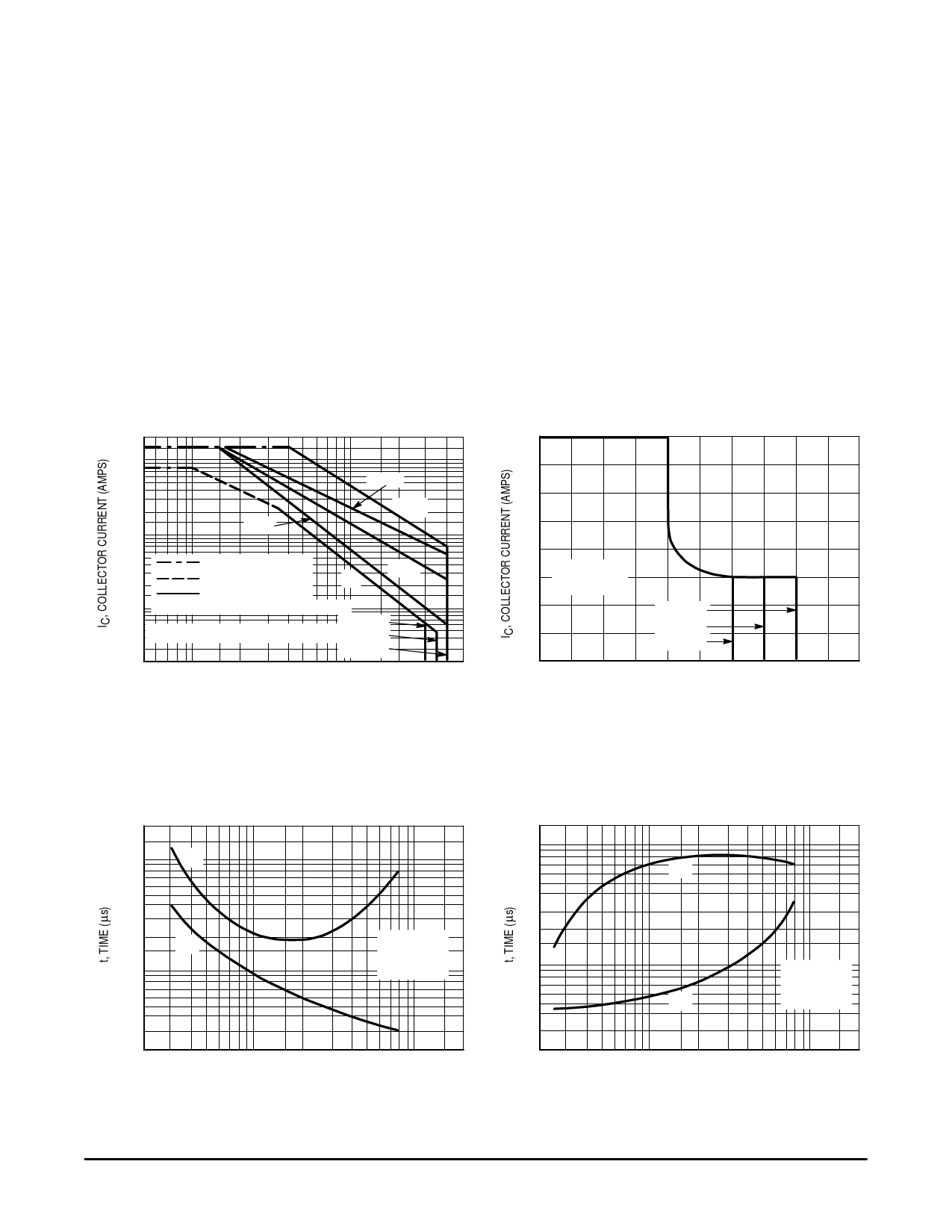
SAFE OPERATING AREA INFORMATION
FORWARD BIAS
There are two limitations on the power handling ability of a
transistor: average junction temperature and second break-
down. Safe operating area curves indicate IC – VCE limits of
the transistor that must be observed for reliable operation;
i.e., the transistor must not be subjected to greater dissipa-
tion than the curves indicate.
The data of Figure 6 is based on TC = 25_C; TJ(pk) is
variable depending on power level. Second breakdown pulse
limits are valid for duty cycles to 10% but must be derated
when TC ≥ 25_C. Second breakdown limitations do not der-
ate the same as thermal limitations. Allowable current at the
voltages shown on Figure 6 may be found at any case tem-
perature by using the appropriate curve on Figure 1.
REVERSE BIAS
For inductive loads, high voltage and high current must be
sustained simultaneously during turn–off, in most cases, with
the base to emitter junction reverse biased. Under these
conditions the collector voltage must be held to a safe level
at or below a specific value of collector current. This can be
accomplished by several means such as active clamping,
RC snubbing, load line shaping, etc. The safe level for these
devices is specified as Reverse Bias Safe Operating Area
and represents the voltage–current condition allowable dur-
ing reverse biased turnoff. This rating is verified under
clamped conditions so that the device is never subjected to
an avalanche mode. Figure 7 gives the complete RBSOA
characteristics.
The Safe Operating Area figures shown in Figures 6 and 7 are specified ratings for these devices under the test conditions shown.
16
10
8
100 µs
3
10 µs
5 ms
1
0.5
0.3
BONDING WIRE LIMIT
1 ms
THERMAL LIMIT
dc
(SINGLE PULSE)
0.1
SECOND BREAKDOWN LIMIT
0.05 CURVES APPLY BELOW RATED VCEO
MJE5742
MJE5741
MJE5740
0.02
5
10
20
50
100
200 400
VCE, COLLECTOR–EMITTER VOLTAGE (VOLTS)
Figure 6. Forward Bias Safe Operating Area
16
14
12
10
8
6
VBE(off) ≤ 5 V
TJ = 100°C
4
MJE5742
2
MJE5741
MJE5740
0
0
100
200
300
400
500
VCE, COLLECTOR–EMITTER VOLTAGE (VOLTS)
Figure 7. Reverse Bias Safe Operating Area
RESISTIVE SWITCHING PERFORMANCE
1
tr
0.7
0.5
0.3
0.2
td
0.1
0.07
0.05
VCC = 250 V
IB1 = IB2
IC/IB = 20
0.03
0.02
0.2 0.3
0.5 0.7 1
2 3 5 7 10
IC, COLLECTOR CURRENT (AMPS)
Figure 8. Turn–On Time
10
7
ts
5
3
2
1
0.7
0.5
0.3
0.2
0.2 0.3
VCC = 250 V
IB1 = IB2
tf
IC/IB = 20
0.5 0.7 1
2 3 5 7 10
IC, COLLECTOR CURRENT (AMPS)
Figure 9. Turn–Off Time
4
Motorola Bipolar Power Transistor Device Data
Share Link: 